Because of the holidays, TI E2E™ design support forum responses will be delayed from Dec. 25 through Jan. 2. Thank you for your patience.

This thread has been locked.

If you have a related question, please click the "Ask a related question" button in the top right corner. The newly created question will be automatically linked to this question.

OPA4187: weird noise on multichannel temp data acquisition system

Part Number: OPA4187
Other Parts Discussed in Thread: LM4040, MUX36D08, , ADS8318, REF5020, OPA4192

Unexplained noise showing up in multichannel temp data acquisition system. Advice sought.

Background:

All bridge, ADC reference voltages generated from amplified 0.1% tolerance TI LM4040 2.048V precision reference. Bridge reference voltages +/- 4.096V. ADCreference 4.096V. Cross couple diff amp pair common mode reference voltage = 2.048V. 

Fully balanced circuit using bridges with ntc thermistors as the sensors.

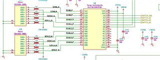
16X sensors signals multiplexed via 2X TI MUX36D08 multiplexers.

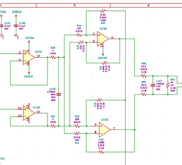
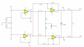
The mux 's are followed by OPA4187 opamps in instrumentation amp configuration and utilizing a pair of cross coupled differential amps (all 0.01% resistors), gain of 0.5. The positive and negative outputs have common mode voltage of 2.048V and can swing between 0-4.096V.

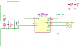
ADC's input antialiasing filter consists of a balanced differential filter. There is series 24.9 ohm resistors and a 1nF COG cap in parallel with 2k ohm.

Sample rate well under 1MHz...around 500kS/s if I recall correctly.

Precision reference, MUX's, opamps, ADC's all running from clean linear regulated +/- 5V rails.

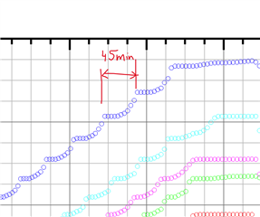
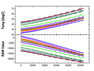
Attached is a screenshot of the temp data taken by our product using this data acquisition circuit described above. Notice the scalloping in the data at higher temperatures and the very long time scale the occur within. I am at a loss to explain why this is happenning.

Could this be some artifact of the temp compensation choppers/servos in the opamps?

What in the world is going on here?
  • Darn. I forgot to mention the ADC part number...it is the ADS8318.

  • Hi Kevin,

    I think what we are seeing is that the voltage at the ADC sample-and-hold input is not settling within the acquisition time.

    The ADS8318 is a 16-bit 500-Ksps SAR ADC which requires a ~10MHz driver to settle within 1LSB in the unipolar configuration. The OPA4187 is a zero-drift amplifier optimized for DC precision with a bandwidth of only 550kHz. Something like OPA192 10MHz amplifier should be configured as an additional buffer stage to drive the ADC.

    In addition to the bandwidth limitations, it is likely that the amplifier is unstable driving a 1nF capacitor with only 24.9Ω of series resistance. Any oscillations at the ADC charge bucket will further reduce the settling performance of the system. The RC filter at the input of the ADC should be tuned for both ADC settling and op amp driver stability.

    Can you provide a schematic? I appreciate your detailed description but a schematic will be very helpful for me to accurately diagnose the issue and provide a solution. I would also like to take a closer look your INA configuration and ADC reference voltage.

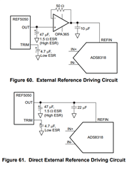
    It is possible that the low-power LM4040 is not adequate to directly drive the ADC reference which will add even more settling error. We can look at using another amp to buffer the LM4040 reference, or perhaps instead using REF5020 which is recommended in the ADS8318 datasheet.

    Please provide a detailed schematic and we will continue the conversation next week.

    Enjoy your weekend,

    Zach

  • Hi Zach,

    Thanks for the reply. I will need to verify the exact sample rate with the Firmware programmer when they return from vacation next week.

    I will post a schematic we did in Kicad. Some of the symbols generated in house may not conform to exact industry standards but but should illustrate the circuit well enough.

    Have a good weekend too.

    Kevin

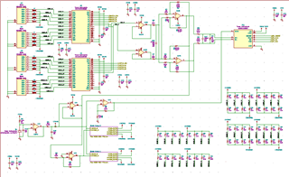
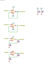
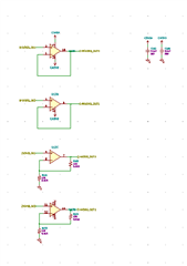
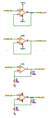
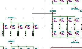
  • Hopefully these show up clearly. All opamps are OPA4187 but not labelled as such. R36 and R37 are zero ohms and C137 is not populated. Sheet Group 0 &1 are hierarchy blocks hiding sub sections of the schematic which are also posted below.

  • sorry this is so hard to read. I can post zoomed in shots per request. If anybody is interested please ask for a zoomed closeup of a specific portion of the schematic.

  • Hi Kevin,

    Yes these are very difficult to read. Are you able to provide a higher resolution image?

    It might help to send multiple images zoomed into the various circuit blocks.

    For example,

    Image 1: Input and multiplexers

    Image 2: OPA4187 front-end

    Image 3: ADC and charge bucket

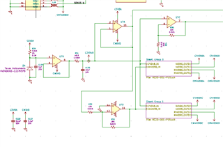
    Image 4: Voltage references and drivers

    The clearer you can get it the better, but as long as I am able to make out the text I will be happy.

    Thanks,

    Zach

  • sorry about the delay. more info after talking to the firmware coder....

    Sample rate is 3.072kHz total and so 192Hz per channel. Also the firmware does a 12 sample average and so the effective data rate is 12Hz/channel after sampling.

    Here are some zooms of the requested sections. Hopefully these show up well enough the rest can be inferred but if you need more please ask.

  • Hi Kevin,

    Thanks for sending the additional information. 

    I see you have your OPA4187 (U10) in a differential buffer configuration with an output common-mode voltage set to 2.048V. Depending on your input common-mode voltage, the output may not be able to swing to 4.096V, as the OPA4187 has a common-mode input limitation 2V below the positive rail. Can you confirm your input common-mode voltage is ~0V? What is the max differential voltage of your input signal?

    3.072kHz is a very low sample rate, so the OPA4187 should be more than capable of settling to 1 LSB within the acquisition time. However, R58 and R59 should be increased to 499Ω for stability.

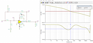
    Is U7 also OPA4187? I notice U7B is driving a 10μF load (C135) with a 50Ω isolation resistor, resulting in a phase margin of only 21 degrees. A minimum phase margin of 45 degrees should be targeted for stability.

    I don't believe C135 is necessary at the output of U7B, as it seems that this node is simply being buffered by U7A and U7C. I recommend removing C135 unless it is providing some function that I am missing?

    A large 10μF-22μF capacitor is necessary at the output of U7C (ADC Vref Pin) to help provide charge directly to the reference pin of the ADC during conversion. I believe this may have been the original intention of C135?

    Please confirm if U7 is OPA4187 or some other op amp as this will affect the stability analysis as well as the conversion accuracy of the ADC. Once I know the op amp selected for U7, I will be able to provide further recommendations for the reference driver circuit.

    Regards,

    Zach

  • Hi Zach,

    Thanks for the replies. Good stuff.

    All the opamps are OPA4187's.

    The input s common mode voltage are indeed at 0V. The bridges are each driven by +/- 4.096V "rails" generated by some of the OPA4187's.

    Our products temp rated exposure extremes are well within the bridges capacity to ever approach the input common mode limit of the opamp.

    As an experiment I might try a larger isolation resistor than 50 ohms and removing C135 if you thought it might help. 

    Best regards,

    Kevin

    Edit missed one: could increase 24.9's to 499's and try that too.

  • Hi Zach,

    Thanks for the replies. Good stuff.

    All the opamps are OPA4187's.

    The input s common mode voltage are indeed at 0V. The bridges are each driven by +/- 4.096V "rails" generated by some of the OPA4187's. the bridges are made up of ~3kohms elements with one of the elements thermistor.

    Within the products rated temperature extremes, the differential input voltage will always be well away from the input common mode limit of the opamp.

    As an experiment I might try a larger isolation resistor than 50 ohms and removing C135 if you thought it might help. 

    Best regards,

    Kevin

    Edit missed one and clarified what I meant a bit above:...... could increase R58, R59 from 24.9's to 499's and try that too.

  • Hi Kevin,

    Yes, removing C135 and increasing R58 and R59 to 499Ω will be necessary, however I still see some issues in your reference driver circuit that will need to be addressed.

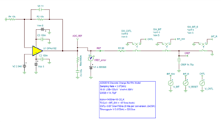
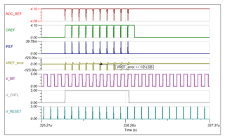
    Although your sample rate is very low, the acquisition time is still 1400ns in which time 16 bits need to be resolved. You will need add a 22μF capacitor at the ADC reference pin to help provide charge during the acquisition. Otherwise the amplifier alone is not able to keep up with the relatively large current pulses occurring every ~88ns, and the reference voltage will droop causing errors. You can test this by probing the ADC Vref pin during acquisition. The goal is for the reference voltage to settle within 1 LSB error before each bit conversion.

    A small amount of resistance in series with the 22μF cap is required to stabilize to reference driver, however this should be kept small to prevent additional voltage errors. The OPA4187 requires an isolation resistor on the order of 100s of Ωs in or to drive a 22μF load.

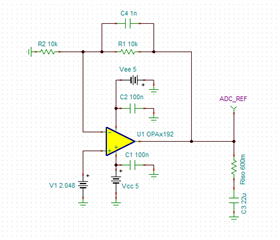
    Instead, I recommend replacing U7 with a faster reference driver that is better suited for capacitive loading, and will allow the reference voltage to settle properly during acquisition. The OPA4192 is a quad 10MHz amplifier with very low offset voltage and offset drift. It is also available in the same SOIC and TSSOP packages as the OPA4187.

    https://www.ti.com/product/OPA4192?keyMatch=OPA4192&tisearch=search-everything&usecase=GPN-ALT 

    See the proposed schematic below for U7C using one channel of OPA4192.

    The 0.6Ω resistor and 1nF feedback capacitor are optimized for stability and settling time.

    Simulation shows that the reference voltage settles well within 1 LSB error within each bit conversion.

    Regards,

    Zach

  • Thanks Zach. Much appreciated. If you don't mind me asking...what is the simulation software you used to generate the bode plots in your earlier post. Neat trick.

    Best regards,

    Kevin

  • Hi Kevin,

    I just used Texas Instrument's Spice simulation tool TINA: https://www.ti.com/tool/TINA-TI 

    If you're interested, this video in the TI precision Lab's series on stability explains how to use TINA to generate these types of plots for stability analysis.

    https://ti.com/video/4080288067001

    I would recommend going through all 7 videos covering stability. These and the other TIPL videos are a great reference for all things op amps!

    Regards,

    Zach

  • Awesome! Thank you. Have been meaning to learn some TINA.

  • Happy to help. Let me know if you need additional support for your design.

    Thanks,

    Zach