This thread has been locked.

If you have a related question, please click the "Ask a related question" button in the top right corner. The newly created question will be automatically linked to this question.

THP210: Poor Total Harmonic Distortion Performance

Part Number: THP210
Other Parts Discussed in Thread: OPA1637,

Hello all,

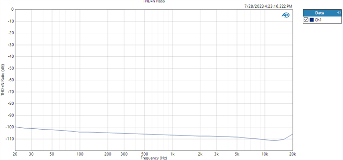
I am trying to get my THP210 design working. For some reason I get poor THD+N values measured with an Audio Precision analyzer. 

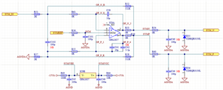
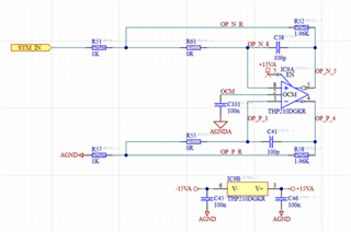
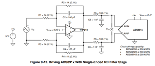
At first I had a gain configuration of 0,135. Assuming it had something to with low gain, I´ve tried a lot of different configurations. At this point I'm just trying to get it working, so I changed my design like Figure 9-12 in the THP210 datasheet (chapter 9.2.2). The THD+N values I get are around -75dB, while my input signal has -113dB. Defaullt input level is 1Vp. I've performed amplitude (10Vp to 10mVp) and frequency sweeps (20Hz to 20kHz), but show no changes to distortion. Differences between the design in the datasheet and mine:

  1. I have VCOM of mid-supply (decoupled with a 100nF X7R capacitor), instead of a Vocm of 2,25V.
  2. Dual power supply of +/-15V (generated by low noise LT3042 and LT3093), instead of a single 5V supply. 
  3. I disconnected resistive load and capacitance from the THP210 outputs. I've measured directly at the output and also with a 100R resistor, to avoid probe influences. Both show the same distortion values.
  4. My feedback resistors are 1.96k instead of 1k. 

I've also tried to "play" with the PD pin. Connecting to GND during startup and to Vcc after supplies have bootet. No effect. Power supplies boot symmetricly.

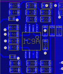
At this point I built the design on a bread board to avoid influences from the rest of my board.

In case it's a batch related issue, the marking on the chip (THP210DGKR) is: 

Top: TI29 1237 

Bottom: 29A P1VE

Am I missing something obvious?

  • HI Jordy,

    - Can you kindly confirm the feedback capacitor part number used in this circuit?  On applications requiring low distortion, it is important to use good quality capacitors on the signal path.  A general recommendation is to use NP0/C0G ceramic or Polypropylene film capacitors in the signal path, and thin film surface mount resistors for best linearity and lower distortion.  Among ceramic capacitors, the C0G/NP0 grade offer the lowest voltage coefficient dielectric and the best capacitance precision. The type of dielectric used in COG (NPO) ceramic capacitors provides the most stable electrical properties over voltage, frequency, and temperature changes.

    It is not uncommon to see THD degradation to the -60 or -80dB level when using lower grade ceramic (non C0G/NP0) capacitors. Attached is a couple of articles discussing the topic.

    Selecting Capacitors to Minimize Distortion in Audio Applications

    Signal distortion from high-K ceramic capacitors

    If you have are already using high grade capacitors, please let me know.

    -  Just to ensure I understood correctly, the set up above also includes 100-Ω series resistance with OUT+ and OUT- to isolate the capacitance of the cable.  Is this correct?

    -  How many devices tested show the high-distortion?  Can you kindly post a  PCB layout?

    Thank you and Kind Regards,

    Luis

  • Hi Luis,

    Thank you for your quick response.

    Regarding the capacitor, I will validate next week for the 100pF. I have tried no capacitance and higher capacitance from 220pF to 5,6nF C0G, but the distortion did not improve.

    ust to ensure I understood correctly, the set up above also includes 100-Ω series resistance with OUT+ and OUT- to isolate the capacitance of the cable.  Is this correct?

    Correct. These 100R resistors are thick film 1%. Before and after the resistor I am measuring the same distortion.

    How many devices tested show the high-distortion?  Can you kindly post a  PCB layout?

    I've had this issue with multiple channels. At least 4. I haven't tested all my prototypes yet. At the beginning I designed the OPA1637, but it ran unstable with low gain (0,135) configuration. In the datasheet of the THP210 it was stated explicitly that low gain configurations where possible. In the datasheet of the OPA1637 this was not said, although Table 9-1 shows that a gain of 0,1 is possible. Anyway, I've replaced the OPA1637 with THP210 and tested multiple configurations.

    I am now testing on a breadboard, but it shows the same results. The original schematic and PCB layout:

    On the PCB, the input signal comes from R51A on the rights side of the screenshot. I've soldered R51A directly to R52A, in case the issue was caused by an unsymmetrical layout. The distortion did not improve however. 

    On my current design, I have following changes compared to the schematic above:

    • Power supply is +/-15V, connectly directly (not over R63 and R64) to C45 and C46
    • R56 N.A., C101 to 100nF X7R (to exclude noise coupling for my reference voltage)
    • C38 and C41 to 100pF (I assume C0G, but I will validate next week)
    • R51 and R57 to 980R (1,96k 0.1% parallel)
    • R52 and R58 to 1,96k 0.1%
    • R54 and R60 N.A.
  • Hi Jordi,

    On the bench, I have performed two tests on the THP210EVM measuring THD+N on the Audio Precision, first with the unmodified/default circuit; and then a second test after modifying to the single-ended attenuator configuration above.

    THP210EVM Default Circuit G=1V/V, THD+N Measurement:  

    • Power supply is +/-15V
    • Gain = 1V/V
    • RIN = 2kΩ, RFB = 2kΩ
    • VOCM Mid supply, floating (or GND) with 100nF capacitor
    • VIN = 3-VRMS (fully differential), VOUT = 3-VRMS

    The direct THP210EVM THD+N G=1 results measuring with the Audio Precision are below:

    THP210EVM Modified Attenuator Circuit, THD+N measurement. 

    • Power supply is +/-15V
    • Gain = 1/4-V/V
    • RIN = 2kΩ, RFB = 501Ω, CFB=100pF (C0G/NP0 50V capacitor)
    • Cload = 100pF (C0G/NP0 50V capacitor) on each output
    • VOCM Mid supply, floating (or GND) 100nF capacitor
    • VIN = 12-VRMS (single-ended), VOUT = 3-VRMS (differential)

    After soldering, the board was submitted to a DI Ultrasonic cleaning bath to remove any solder flux. The THP210EVM THD+N Attenuator Single-ended to differential results measuring with the Audio Precision are below, the THD+N changes due to the attenuation and SE to Diff conversion, but THD+N performance is still better than -100dB:

    Suggestions:

    • As we discussed, please ensure to use COG/NPO, high grade, 50V capacitors on the signal path: including inputs, feedback and RC output filters.
    • Important note regarding solder flux: Leakage currents from solder flux contamination can disturb the amplifier's operation, especially when performing sensitive THD measurements. The PCB must be re-cleaned anytime devices are soldered into the PCB.  On our lab, the recommended cleaning procedure requires access to an ultrasonic deionized (DI) water bath:
      • Place the EVM in the ultrasonic cleaner and fill with fresh deionized (DI) water.
      • Run the ultrasonic cleaner for 20 minutes at 45°C.
      • Remove all moisture from PCB.
    • If an ultrasonic bath is not available, then a manual cleaning procedure is possible:
      • Scrub contaminants from the top layer using a brush and DI Water
      • Use a toothbrush to gently scrub for 60 seconds. Focus on sensitive input, feedback and output areas in the PCB. Scrub contaminants from the bottom layer as well. Flush the scrubbed areas with fresh DI water, tilting the board to allow runoff to flow away from the input areas.
      • Remove all moisture from PCB
    • Increase the capacitor value on the VOCM. You may leave this pin floating for mid supply, but use a ~100nF capacitor I close proximity to VOCM
    • If you are not planning to use the PD pin, consider connecting to the THP210 V+ supply
    • If you are planning to revise the PCB board, you may consider improving the symmetry of the positive and negative signal path. To minimize second and other even-harmonic content, route traces as symmetrically as possible for both positive and negative feedback pathways. Place feedback components in close proximity to the output and input pins of the device. For example, consider removing C42 on the design to make the positive and negative feedback as symmetric as possible.

    If you wish, you could also consider using the THP210EVM for preliminary tests.

    Kindly let me know if issues persist.

    Thank you and Kind Regards,

    Luis

  • Hi Luis,

    Thank you for your support. I finally found the issue. It was not related to the THP210. The problem was that I was measuring single ended at the output stage. When I started measuring differentially, my THD+N was at about -110dB. I have yet to figure out why single ended measurement deliver such bad results, but that is not of your concern.

    Once again, thanks for your support and effort.

  • HI Jordy,

    That's good news, Thank you for letting us know,

    Many Thanks,

    Luis