


Other Parts Discussed in Thread: TINA-TI
Hi,
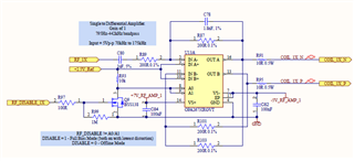
I have the attached circuit built onto a PCB.
It is essentially intended to take a 5V sine wave input of varying frequency, and outputs a differential waveform which applies power over a ~27R load, with a small amount of filtering.
The circuit successfully simulated using the pSpice model provided on the product page, (simulated within altium).
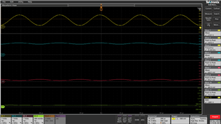
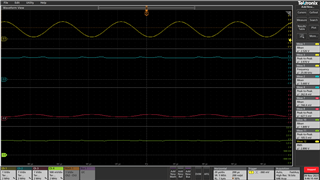
However in reality it appears to output a wave with a tiny amplitude and large DC offset.
Can anyone make any suggestion why I am seeing the results shown on the oscilloscope screenshot, rather than those shown in the simulation?
And what may be done to resolve this issue?
Thus far all I can glean is that my setup of A1/A0 may not be ideal.
(Doesn't seem to drive above 2V as intended. Though does to exceed the absolute maximum of Vee+5, which could be the problem).
How should the bias pins be driven, if a negative supply of under -3V is used?
(If A1/A0 is referenced from GND and requires at minimum 2V for logic 1).
(Scope Screenshot Ch1 - RF_1X | CH2 - COIL_1X_P | CH3 - COIL_1X_N | CH4 - A0/A1)
![]()
Thanks, Andrew

