Because of the holidays, TI E2E™ design support forum responses will be delayed from Dec. 25 through Jan. 2. Thank you for your patience.

This thread has been locked.

If you have a related question, please click the "Ask a related question" button in the top right corner. The newly created question will be automatically linked to this question.

INA849: Schematic review

Part Number: INA849
Other Parts Discussed in Thread: AM6442, OPA388, OPA328, OPA810

Dear team, 

The customer would like to use AD8421, competitor device at current sensor application based on CT. 

I want to replace this device to Our INA849. Please refer to the below schematic. 
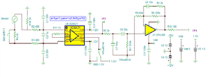
Would you review above schematic? And let me know your opinion regarding INA849 can replace this device on above schematic. 

Do you know what filters the customer has configured from the AD8421 output to the VF4 output? passive component value can be ignored. 

And could you recommend output filter of INA849 to configure current sensing circuit based CT? 

Thank you. 

  • Hi Nam,

    Do you know what filters the customer has configured from the AD8421 output to the VF4 output? passive component value can be ignored. 

    As shown on the schematic above, the INA849 has an input low-pass filter with a corner frequency at ~159-Hz.  The op-amp stage, shows a passive bandpass filter (passive high-pass, and low pass filter RC filter), followed with the amplifier set on a non-inverting gain, low pass configuration. Nevertheless, as shown, the filter frequency response is very low and You have mentioned that the passive component values can be ignored. Do you have an schematic that has the correct filter passive components? Or, alternatively, can you please define what is the CT signal bandwidth of interest, and the filter frequency response characteristic required? 

    And could you recommend output filter of INA849 to configure current sensing circuit based CT?

    This is dependent on the CT signal of interest and bandwidth characteristics.  For example, on CT applications specific to Grid metering power applications, some applications use a low-pass filter, allowing the 50Hz or 60Hz fundamental alternating current signal, plus several harmonics of the fundamental, for example a low pass filter with BW around few kHz of bandwidth. Nevertheless, this can vary depending on the specific CT application above.  Please let us know what signal is used on the CT application above and the bandwidth of interest. If you require us to advise on a filter design, please define the filter type (low-pass or band-pass), filter specification and frequency response characteristic, ie, filter order, filter response characteristics (Butterworth, Chebyshev).

    Would you review above schematic? And let me know your opinion regarding INA849 can replace this device on above schematic. 

    The INA849 is a very low noise device with input referred noise of 1nV/sqrt(Hz) at 1kHz (Gain=1000V/V), wide-bandwidth instrumentation amplifier with 1.25MHz BW at G=1000; hence offering improved noise performance and wider bandwidth, hence it can work well in the application above.   

    One circuit change, the INA849 defines a different gain equation than the AD8421, where the gain of the INA849 is given by:

    INA849 Gain = ( 1 + 6kΩ / RG). 

    If a gain of 762.53-V/V is required as shown on the AD8421 schematic above, the ideal gain resistor value for the INA849 is RG = 7.8787Ω.  For example, you could choose a standard value 7.87Ω resistor for a gain of ~763.3V/V.  If you like us to provide schematic suggestions, we require additional information:

    1) Input common mode voltage range at the INA849 input.  Clarify if the CT is grounded above, it appears R16 is connecting to GND on the sensor but the connection is unclear.

    2) Minimum/Maximum CT current range at the input of the INA849.

    3) CT signal frequency response requirements and filter frequency response requirements. Please define the filter type (low-pass or band-pass), filter order, filter frequency bandwidth specs, and response characteristic (for example, Butterworth response). 

    4) What circuit, or what is the load is driven by the amplifier stage.  If this is an ADC, which ADC device, ADC resolution, ADC full-scale range, sampling rate.

    5) Output voltage range required at the op-amp stage amplifier output.

    Thank you and Regards,

    Luis

  • Hello Luis, 

    Thank you for your comment. Please refer to the below my comment and Please provide schematic suggestions. 

    1) Input common mode voltage range at the INA849 input.  Clarify if the CT is grounded above, it appears R16 is connecting to GND on the sensor but the connection is unclear.

    2) Minimum/Maximum CT current range at the input of the INA849.

    The Current range is 0 to 50A , input range of INA849 is 0~200mV(not fixed) 

    3) CT signal frequency response requirements and filter frequency response requirements. Please define the filter type (low-pass or band-pass), filter order, filter frequency bandwidth specs, and response characteristic (for example, Butterworth response)

    Filter frequency is 200KHz , cut off frequency , filter type low pass filter 

    4) What circuit, or what is the load is driven by the amplifier stage.  If this is an ADC, which ADC device, ADC resolution, ADC full-scale range, sampling rate.

    5) Output voltage range required at the op-amp stage amplifier output.

    The load is ADC, the customer want to use internal ADC of AM6442 device. 12bit, Up to 4 MSPS, full-scale 0 to 3.3V , output voltage range of Op Amp is 0 to 3.3V. and they want to use zero drift amp solution like OPA388. 

    Thank you. 

  • Hello Dino,

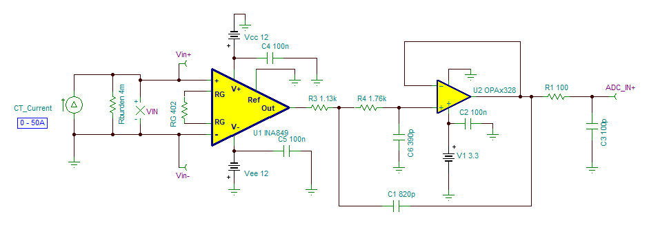
    Since the INA849 input signal is 0-200mV, and the ADC full-scale input range is 3.3V, the INA849 would need to be set on a gain around ~16V/V with a gain resistor of RG=402-Ohms. The circuit assumes that the sensor common-mode voltage is biased at GND, or that the input common-mode voltage is within the linear range of the INA849.

    The circuit above consists of an instrumentation amplifier, set on a gain amplifying the CT signal, followed by a second stage op-amp filter stage driving the ADC. Since the INA849 is a high precision, low drift instrumentation amplifier, set on a gain of 16-V/V, the offset and offset drift performance in the signal chain is heavily dominated by the first instrumentation amplifier gain stage, and the second op-amp stage does not contribute a significant error. Hence, there is no significant benefit of using a zero-drift amplifier such as the OPA388, since the CT signal is already gained up. 

    Also, If you require to support the ADC of the AM6442 device at a high-sampling rate, you will require a relatively higher bandwidth amplifier that offers low closed-loop output impedance at high frequency to be able to drive the 12-Bit SAR ADC sample-and-hold, and settle within the 12-bit ADC resolution during the short acquisition time. Therefore, I do not recommend a zero-drift amplifier for this application.

    One possible circuit is below, using the INA849 on Gain of 16V/V, followed with the OPA328 in a Sallen-Key low-pass filter configuration with a corner frequency around 200-kHz. The sampling rate and/or acquisition period of the AM6442 is programmable, and this circuit will be able to drive the ADC sample-and-hold and settle within 1/2-LSB of the 12-Bit ADC resolution at a sampling rate up to 3.125-MSPS.

    Assumptions on ADC Timing: 

    - ADC sampling rate <= 3.125-MSPS

    -ADC0_SMP_CLK = 60MHz

    -Acquisition Time = 6*ADC0_SMPL_CLK_Cycles = ~100ns

    -Conversion Time =  13*ADC0_SMPL_CLK_Cycles = ~216.7ns  

    If you require to support a faster sampling rate, to maximum throughput of 4-MSPS, you will need a higher bandwidth amplifier such as OPA810; but keep in mind, the minimum supply for the OPA810 is +4.75V.

    Thank you and Regards,

    Luis