Because of the holidays, TI E2E™ design support forum responses will be delayed from Dec. 25 through Jan. 2. Thank you for your patience.

This thread has been locked.

If you have a related question, please click the "Ask a related question" button in the top right corner. The newly created question will be automatically linked to this question.

INA214: INA214 application question

Part Number: INA214

Hi team,

when using the INA214, the input pin IN+ IN- measured the following waveform; our question is that according to the description in the specification, when the default negative voltage is generated, can the current be limited to 5mA by R3 and R4?  and can it be determined to be no risk? Thanks!

  • Hey Dane,

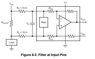
    No. Internal resistors R3 and R4 will not limit current. The image shown is an oversimplification. In reality there are input ESD cells at IN+ and IN- pin and so to limit currents during Vcm violations (e.g., <-0.1V for the INA214B), you will need external input resistors (Rs) as shown in datasheet below:

    To calculate the necessary Rs, use Rs_minimum = |Vcm_max|/5mA. So if Vcm can drop to -2V, then you need at least 2V/5mA = 400-Ω input resistors at each pin. Rs limits the body diodes of the internal ESD cells, which will begin to turn on once negative Absolute Maximum rating is exceeded. 

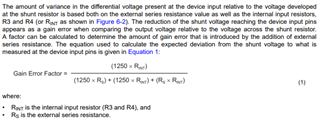
    Since 400Ω > 10Ω, you will see significant shunt voltage gain attenuation. This attenuation factor can be calculated with the equation from datasheet:

    You can refer to this application note and training video for more information on protecting input ESD cells for CSA and for calculating gain error with input resistors here:

    https://www.ti.com/lit/ug/tidu473/tidu473.pdf

    https://www.ti.com/video/6219017476001

    https://www.youtube.com/watch?v=hLGN_wl-xgA 

    Hope this helps.

    Sincerely,

    Peter