Other Parts Discussed in Thread: INA186, INA2191, INA4290, INA280, INA281
Hi TI experts,
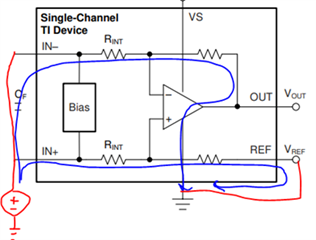
I was using INA4181A2IPWR and found that it has a large power consumption after shutting down. The test is as follows. IN+1 and IN-1 are directly connected to the power supply B+ through RSENSE. It has no MOS tube control and always supplies power to the INA4181A2IPWR input pin IN+1. and IN-1. When testing the system shutdown power, it was found that the IN+1 pin will cause a current of 75uA, which is unacceptable for my product design.
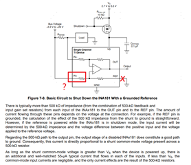
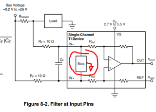
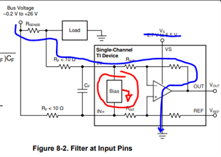
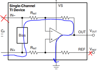
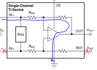
As shown in the attached specification picture, I connected REF to ground and disconnected it, but the 75uA current did not decrease.
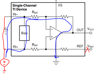
So I want to know if the internal block diagram of the IN+1 pin of this INA4181A2IPWR is equivalent to connecting a 250KΩ resistor to ground? How is this IN+1 pin connected internally? I would like to refer to how to reduce power consumption, or do you have a better solution?