This thread has been locked.

If you have a related question, please click the "Ask a related question" button in the top right corner. The newly created question will be automatically linked to this question.

OPA810: To high quiescent current during overload

Part Number: OPA810
Other Parts Discussed in Thread: OPA2863A, OPA863, OPA828

Hi Team,

We have a problem with too high quiescent current of opa810. 

According to the datasheet, the current consumption of a single amplifier should be approximately 4 mA. Under standard conditions, this agrees perfectly with our observations.

The problem appears at higher input voltages, and especially, as we assume, at overdrives. The current consumption can then increase to up to 20 mA per amplifier. How to explain this phenomenon?

Our design is battery-powered, and we were a bit surprised by such a current consumption. By isolating fragments of a larger circuit, we have determined that the culprit was the input stage in a classic instrumentation amplifier configuration:
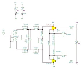
Problematic part

The resistance at the output of the amplifiers, as given in the diagram, is 3 kOhm. The output voltage level is +-9V. This gives an output current of 3 mA max. When added to the power supply current of the amplifiers, it theoretically gives a maximum of approximately 12 mA. When the amplifiers are overdriven with a constant signal, the current consumption of this part of the system coincides with these calculations and is about 15 mA. Increased consumption appears when an AC overdrive occurs and depends on the frequency of the overdrive. When we overdrive the system with a sine or square wave with a frequency of 1 MHz, the current consumption increases up to 43 mA (we suspect 20 mA for each amplifier + 3 mA for the amplifiers' output current).

The device is designed carefully, the noise and attenuation of the common signal (of the entire system, not only the parts from the diagram) are within the design limits (250 uV at output at 20 dB gain, CMRR > 60 dB for 1 MHz). There are no excitations, especially oscillations on the signal edges (checked up to 200 MHz). The distorted output signal has the shape that one would expect - with just clipped peaks:

1 MHz with overdrive

Apart from increased power consumption, nothing bad happens. Simulations in Tina software do not show increased power consumption. Generally, they slightly underestimate the consumption, because they give it at the level of 10 mA (the entire part of the system) for full overdrive. 

Can overdrive recovery state result in such an increased power consumption? Isn't this harmful to the amplifiers?

Regards,

Marcin

  • Hi Marcin,

    When an amplifier is overdriven on the output (and output is saturated), an input differential voltage greater than the typical offset appears between the inputs, which triggers the slew boost circuit thus increasing the quiescent current. An increased current is also drawn in the output stage to nullify this input differential. This behaviour is characteristic of any rail-to-rail output amplifier with bipolar output stage.

    Since this increase in Iq is an issue for your system, you should consider using amplifiers with overload power limit, such as the OPA2863A. This device has an overdrive monitoring circuit which limits the slew boost and output stage current during overdrive conditions and keeps the Iq to only 1.4mA during such conditions. That said, the OPA2863A needs a higher 300 nA bias current on its inputs which is greater than the pA bias currents on the OPA810. 

    Could you consider using the OPA2863A in your application?

    Regards,

    Bharat Agrawal

  • Hi Bharat,

    Thank you for the quick reply. Opa863 was our first choice. Everything was fine except for the slightly too low max. supply voltage. It was critical at the input stage of the device.

    I still have questions about the opa810. As I understood, the slew rate booster detects the difference between the inputs exceeding a certain threshold (larger than the offset). I accept this, but why is there no increase in current consumption with static overdrive? Does the system additionally differentiate this information to work only for signal edges?

    And the most important: As I understand it, this is a normal operation of this amplifier and does not pose a threat to it even with long-term activation with an alternating (sinus for example) waveform? It seems that increasing the power lost per amplifier to about 400mW should not be dangerous, but are there no other threats?

    Regards,

    Marcin.

  • Hi Marcin,

    The additional power consumption with sinusoidal input/output (with clipping) is also due to the large signal rail-to-rail slewing of the output where the slew boost is also active in linear region and draws a higher Iq from the supply rail to boost the diff pair tail current and enable such large signal swings. Higher the frequency this Iq will increase furthermore due to repeated slewing for rail-to-rail output and higher Iq being drawn in each cycle.

    About the reliability, nominally this doesn't pose an issue but for 400mW dissipaton the ambient conditions will need to be considered (ambient temp, air flow and cooling availability etc.). The best thermal performance is offered in the SOIC-8 package with Rtheta-JA of 134.8C/W hence once could expect a die temperature delta of ~54 degC from ambient which can cause a failure in absence of forced cooling.

    An alternate option which could be considered is the OPA828 which is a 45 MHz GBW, 36V FET input amplifier with overload power limit. While this does meet your supply voltage requirements, it is not rail-to-rail input or rail-to-rail output for which you will need to adjust the supply voltages if +/-9V is needed at the output.

    Regards,

    Bharat agrawal

  • Hi Bharat,

    Rail-to-rail input and rail-to-rail output are crucial to our project. We checked this earlier and the opa810 is the only amplifier that meets the conditions. We also considered the opa828, but rejected it due to significant limitations of the common mode voltage (even 3.5 V to V+) and, paradoxically, due to its higher current consumption than the opa810 (5.5 mA vs 3.7 mA).

    We are only sorry that the opa810 data sheet does not clearly indicate that it has a slew rate booster and that it can increase the current consumption so drastically (up to five times) in certain conditions.

    As we have checked, large signal driving of the opa810 itself does not increase the current significantly. The key is to frequently bring it into a state of saturation/overdrive. It seems that the slew rate booster is not activated to a significant extent during normal operation (even with large amplitudes and high freq.), but only during overdrive. This may be related to the adaptation of the opa810 to work with a multiplexer at the input (as mentioned in data sheet). Either way, we would like to point out that the data sheet for the opa810 could clearly address this issue - clearly point to the existence of a slew rate booster and warn against a possible significant increase in current consumption, an increase so large that it should be taken into account in the thermal design.

    When it comes to thermal design, it is probably more appropriate to use the RθJB parameter, because we are dealing with an SMD package. This parameter is the worst for SOIC. We used SC70, because only this package gave us good path routing ensuring low capacitances and exemplary behavior in the required frequency range, including the extensive gain switching system. The RθJB for SC70 is 69C/W, which would give a die temperature delta ~27degC. Of course, it is difficult for us to apply the ideal case (69C/W) to our PCB design with a small amount of copper surface, but fortunately the PCB is relatively large and not intensively packed with elements :), so there is the chance that thermally opa810@sc70 will survive. It is important that no overdrive should occur during assumed normal use. We tested this case just in case.

    In summary,
    we interpret the information to mean that the operation of the amplifier (with increased current consumption) is consistent with its design, more, the significantly increased current consumption is intended by design, although it is not described in the data sheet.
    This is not a sign of amplifier malfunction or our design errors and this is not dangerous to the system in any way other than thermal. If we are wrong, please let us know.

    We consider your informations to be highly important and useful, especially for future projects, and thank you again for your quick response.

    Despite the unexpectedly increased current consumption, we still consider the opa810 to be an extremely interesting amplifier, even one of a kind.

    Regards,

    Marcin

  • @Marcin , I will let Bharat / Apps team answer the question you pose since they are in loop .

    My name is Shree and I work as a product definer for High Speed Amps .

    We are developing a next gen OPA810 called the OPA811 which solves this issue , has lower noise and better precision. Is it okay to have quick chat for 15 mins / 30 mins to understand the requirement here so as to help with us with an upgraded product of OPA811 and ensuring it fits your system perfectly.

  • @Shree, Sure, with pleasure. Just let me know when, because we're probably in very different time zones.