Because of the Thanksgiving holiday in the U.S., TI E2E™ design support forum responses may be delayed from November 25 through December 2. Thank you for your patience.

This thread has been locked.

If you have a related question, please click the "Ask a related question" button in the top right corner. The newly created question will be automatically linked to this question.

OPA818: TINA-TI Simulation and Physical Test Results Are Different

Part Number: OPA818
Other Parts Discussed in Thread: LMP7717, TINA-TI

Dear Engineers,

We want to design a transimpedance amplifier with a gain over 1G V/A, and we also want its bandwidth to be as high as possible. We already know the impact of input capacitance and feedback capacitance on the circuit, and the parasitic capacitance of high-resistance feedback resistor will play the same role as the feedback capacitance. Therefore, we learned the design methods of some papers and improved the feedback loop.

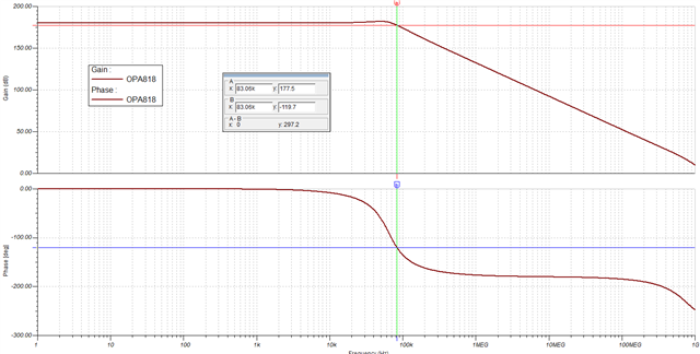
We found that the TINA-TI simulation results of the improved circuit show that the OPA818 should perform better than the LMP7717, but in actual testing the LMP7717 can achieve higher bandwidth(about 20KHz).
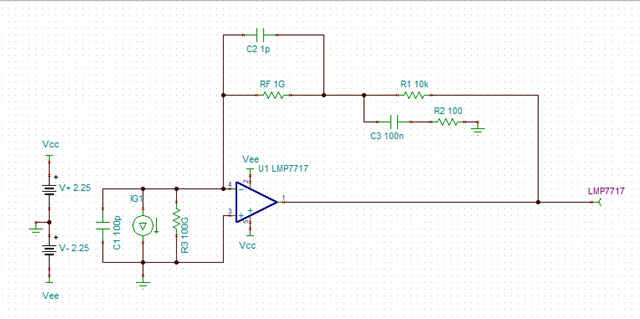
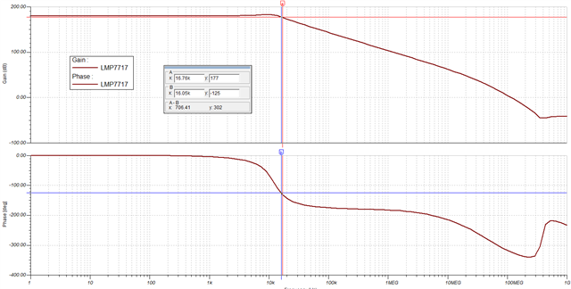
Our TIA Circuit

Bode-LMP7717

Bode-OPA818

Our question is:
1.How to explain the contradiction between simulation and physical experiments?
2.Is the parasitic capacitance of the 1G ohm feedback resistor 1pF? (Because it is difficult to measure the actual circuit, we have to estimate it)
3. Is OPA818 the best chip we should choose?

These are our file:

/cfs-file/__key/communityserver-discussions-components-files/14/4812.opa818.TSC

/cfs-file/__key/communityserver-discussions-components-files/14/2364.lmp7717.TSC

Thanks for your help

  • Hi Shuzheng,

    I was able to look over the circuits you provided and there is a chance the circuit is having some stability issue when adjusting the circuit. The typical parasitic capacitance of a SMD resistor is usually estimated to be from 0.1pF to 0.2pF. When adjusting for this in the simulation for C2, you do get significant peaking, which is a sign of a stability problem in the system. I assume C2 is not a real component in the circuit, if so, are you seeing any peaking in the response of the circuit? Could you also provide the bandwidth captured for the real-world measurement for each circuit. When comparing the layouts for the circuits, are they very close to each other? Any additional parasitic capacitance that one layout might have versus the other will affect results as well. As for the chip selection, it is very interesting the slower device is performing better unless there is something else being affected that simulations cannot capture. However, to answer your question, major differences in simulation versus real life measurements especially with higher speed parts is the parasitic capacitance that will exist in a real-world circuit. If has a major impact on performance and it is something simulation does not capture. In general, our models also do not capture distortion and more of the non-linear behavior that a device would exhibit in real life as our models are not transistor based. 

    Best Regards,

    Ignacio

  • Thanks for your reply!

    We do see spikes in the output response in real-world testing. Fortunately, this situation can be improved by adjusting the circuit design.
    Using square wave signals for testing, the measured bandwidth of LMP7717 can exceed 20kHz, but the bandwidth of OPA818 is only about 1kH.
    Your answer has inspired us a lot. We will try our best to ensure that the PCBs of the two chips are consistent and retest (the two circuit boards tested before were not completely consistent).

    Finally, I saw that there is a view that the input impedance of high-speed operational amplifiers is not high, which may have some impact when the transimpedance is high. What do you think? Are there factors other than GWP that affect circuit performance?

  • Hi Shuzheng,

    If you are seeing peaking in your real-world responses, there is a chance you are seeing higher bandwidth in the slower device because the peaking is slightly extending the bandwidth, but this is not an ideal circumstance. When using our TIA calculator (attached below) you can see that the required feedback capacitor at this high of a gain would be a few femtofarads which is not a realistic value. For a gain this high it is recommended to split the overall gain into multiple stages as a single gain stage like the current design is likely not feasible. As for your question, one big concern in a really high gain (large RF) is the impact this will have with the ib current of the amplifier as this ib current will interact with the large Rf resistor and create an offset. Therefore, for any circuits with very large Rf values, we recommend using an amplifier with a fet input stage. This fet input stage is very high input impedance compared to a bipolar input stage and will result in a small ib current which is magnitudes lower than a bipolar input stage. So, the input impedance of a device is not dependent so much on its speed but more on its internal input stage architecture. As for your design it will be recommended to use devices with a fet input stage like the OPA818 you chose. 

    Best Regards,

    Ignacio