


Part Number: LM7171
Hi all,
I'm looking at the LM7171A and need some clarification from the datasheet.
I suspect that there is a difference between the A and B version of the LM7171 (regarding the input offset voltage drift).
If you take the specification from the datasheet: TCVOS: 35uV/C and compare this to the 2 figures in the datasheet:
If you take the specification from the datasheet: TCVOS: 35uV/C and compare this to the 2 figures in the datasheet:
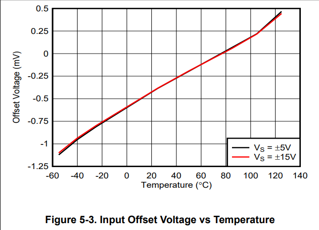
Figure 5-3 (LM7171A) Input Offset Voltage vs Temperature, calculating the drift from this (+-15V): -40C=-1mV and 100C=0.2mV. This gives 1.2mV / 140C = 8.5uV/C
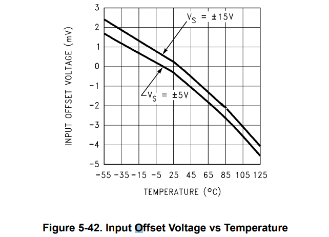
And figure 5-42 (LM7171B) Input Offset Voltage vs Temperature, calculating the drift from this (+-15V): -35C=2mV and 125C=-4mV. This gives 6mV/160C = 37.5uV/C
Given the large difference between the calculated value and the spec given on page 4 (TCVOS): Is this spec only applicable for device B or both A and B?
What is the correct drift specification for device A? The graph or the number given in the datasheet?
Thanks in advance!
