Hi all,
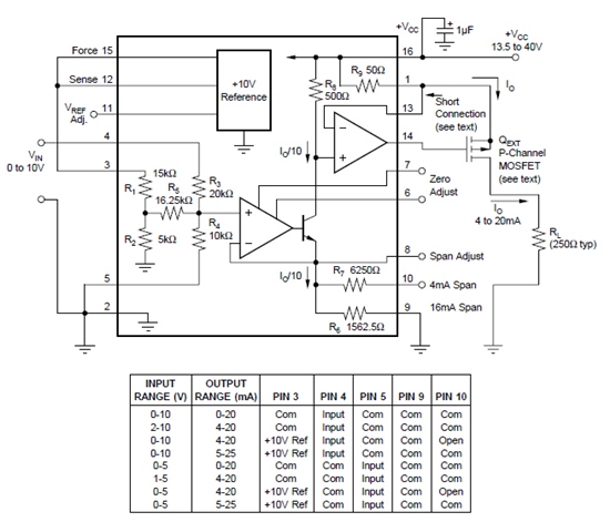
I'm trying to use XTR110 for converting 0-10 V DC to a 4-20mA current loop.
When I tried it with the exact circuit given in the datasheet the pin no. 14 shows 1.344V irrespective of the input voltage.
Please help me out.........
This thread has been locked.
If you have a related question, please click the "Ask a related question" button in the top right corner. The newly created question will be automatically linked to this question.
Hi all,
I'm trying to use XTR110 for converting 0-10 V DC to a 4-20mA current loop.
When I tried it with the exact circuit given in the datasheet the pin no. 14 shows 1.344V irrespective of the input voltage.
Please help me out.........
Hello Shrikant,
The pin 14 voltage of 1.344V tells me much other than that the device is trying to turn the PMOS "ON" as hard as it can by creating a very large Vgs voltage.
Are you sure you have the circuit connected as shown below? The PMOS must be connected for the circuit to function properly, have you verified your transistor is properly connectioned?
Please be sure your power supply voltage is between 13.5 and 40V. A good indicator that the device is powered approrpriately is to verify that the +10V reference is at the correct voltage.
For 0-10V input and a 4-20mA output, please verify that your circuit matches the image below.

Please try the above suggestions and post an update if you need further assistance.
Best Regards,
Collin Wells
Precision Analog
Hello Collin
I'm sorry for being late on this but m glad that the circuit has started working with very good accuracy.
As recommended in datasheet all the returns i.e; grounds should be connected common as nearest as possible to pin no. 2.
When I connected all the grounds at pin no. 2 (GND) I found ckt working properly but m not sure whether because of this only the circuit was not working properly.
I couldn't understand the exact concept behind making only one common point for all returns, and m confused whether I should use ground plane for rounting the PCB or not.
Thanks again for quick reply.
Thanks and Rrgards
Shrikant Lokhande
Design Engg.
Symtronics automation.
Hello Shrikant,
The purpose of trying to connect all of the returns to the same connection near pin 2 is to ensure that the return (GND) voltage that the input and output circuits are referenced to are at the exact same potential. This prevents a PCB related offset from being induced between the two potentials causing an offset/error on the output.
Unless you previously had an open/bad connection, changing the GND signals to connect at pin 2 should not have fixed the issue you were previously describing. It would only improve performance on a poorly operating circuit, it would likely not fix a non-functional circuit unless the previous GND scheme was extremely poor.
You can and should use a GND plane for your circuit routing. However, be aware where your GND return signals actually are and be sure that the path of least resistance will lead the GND returns back to the same potential as pin 2.
Please let me know if I can clarify anything further.
Best Regards,
Collin Wells
Precision Analog
Hello Collin,
Thanks for the clarification. Actually I have built the circuit on general purpose PCB so there are some chances of bad grounds or dry soldering.
As per my understanding the input pin (pin no. 4) should show 0V reading for no input or zero setting condition but in my circuit it shows 0.814 volts when input is disconnected and this results in to o/p current to get to 5.2mA. I used trim pots for this but the offset remains their. As soon as I connected input it was showing proper readings.
I believe this is because of grounding only but would like to ask you whether there are any other reasons for this.
Thanks and regards,
Shrikant
Hello Shrikant,
It seems that the floating input is picking up stray noise. Can you try connecting a 0.1uF capacitor between input and ground and revert with the results?
Regards,
JayantD
Hello Shrikant,
A low pass RC filter at the input will help. e.g. 47k, 0.1uF etc.
Regards,
Jayant
Hello Sir,
Thanks a lot for the suggestions, I tried RC filter but it didn't work for my circuit.
Then I used 4k7 pull down resistor, the offset went to a negligible value and got 4.05mA o/p at zero condition.
Thanks and Regards
Shrikant
Hello,
Thanks for your comments Jayant!
Shrikant,
The behavior you're experiencing is expected. The input needs to be connected to a low-impedance driver to ensure proper output voltages. So when you need 4mA as the output you must tie the input to 0V, it can not float. The 4.7k pull-down will ensure that the output is close to 4mA when the input is disconnected because it provides a current path to GND.
Please see the circuit below which corresponds to your results. I've attached the simulation file that I used for this test. It is a rough simulation model of the XTR110 and is overly idealized so please be sure you are operating within the datasheet specifications before creating a design using this simulation file.

Best Regards,
Collin Wells
Precision Analog