This thread has been locked.

If you have a related question, please click the "Ask a related question" button in the top right corner. The newly created question will be automatically linked to this question.

TLV1701: Open drain output effect on external RC

Part Number: TLV1701
Other Parts Discussed in Thread: TLV1811, TLV1805,

Hello,

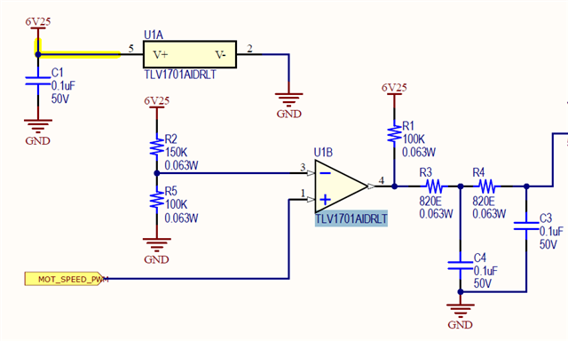
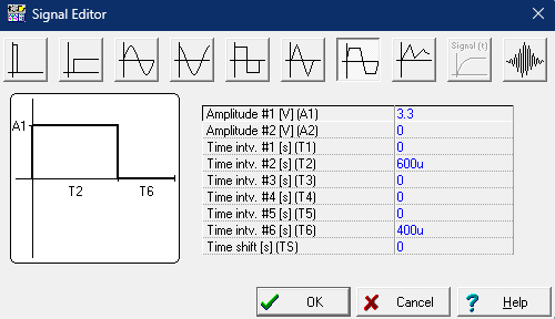
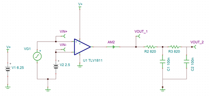
Please find our below circuitry ,

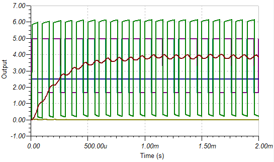
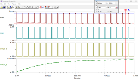
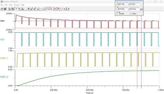
MOT_SPEED_PWM is a 3.3V PWM Signal , we are using opamp for level shifting it to 6.25V keeping 2.5V at reference.

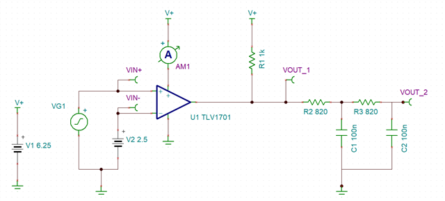
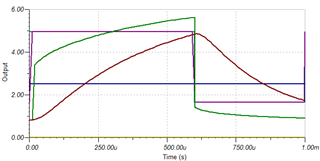
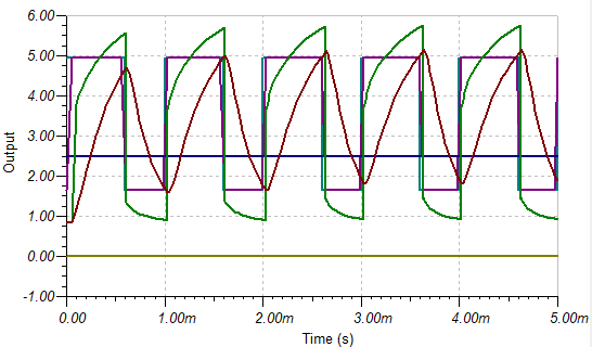
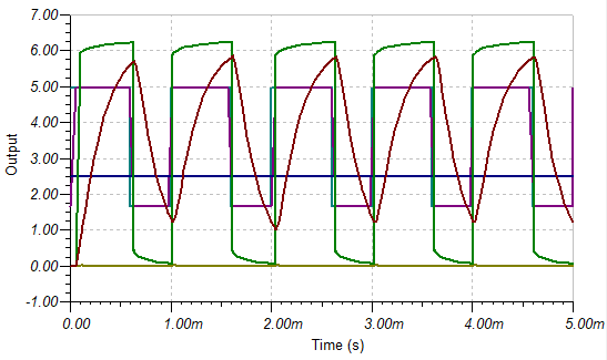
The 6.25 PWM output is later required to convert into DC. So second order RC Filter is used.

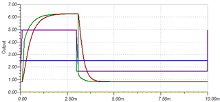
But because of this i am not able to see 6.25V at the output , it is getting dipped down.

As I increase the TON of MOT_SPEED_PWM Signal, Output is getting increased gradually , But this is impacting the rest of the circuitry. Is there are any suggestion for this?

  • You must not use an open-drain output for a PWM DAC. You need a symmetrical push/pull output, e.g., TLV1811 or TLV1805 (they have a different pinout).

  • Hello Celmens,

    Yes, we have a mistake here , Is there any pin to pin compactible push pull comparator for TLV1701AIDRLT?

  • Is there any correlation between Vout and pull up resistor connected along with varying PWM?

    Output seems to be non linear for varying PWM. 

  • There is no P2P device.

    To improve the behaviour, make R1 much stronger (somewhere between 10 kΩ and 1 kΩ). But it cannot be as strong as the comparator's output, so there will still be some nonlinearity. You could try to simulate the circuit, but the easiest way might be to calibrate the PWM-to-voltage relationship with a test circuit.

  • Hi Asha,

    Thank you, Clemens for the information.

    As he mentioned, we currently don't have a P2P device for TLV1701 with push/pull, however making R1 stronger as well as simulation/testing will improve performance.

    Regards,

    Michael

  • Thanks for the response.

    Could you please help me generate PWM with diff duty cycle and frequency in Tina TI as this part is available only in Tina TI to try simulation.

    I am not able to generate PWM signals from the voltage generator as we do in LTspice. Could you please support!

  • Sure thing. I setup a TINA circuit according to your layout with a 1k ohm PUR.

    Setting up a PWM with different duty cycles isn't intuitive in TINA, but you can use a general waveform and use the time intervals to create a PWM signal. For example, this creates a 30% duty cycle at 100 Hz on In+ using the voltage generator:

    Vout_1 is the green waveform and Vout_2 is the red waveform.

    or a 60% duty cycle at 1kHz:

    Please let me know if you'd like a specific set of frequency/duty cycle PWM signals, or how I can be of further assistance.

    Attached is this TINA file as well.

    4135.TLV1701.TSC

    Regards,

    Michael

  • I am in need of continuous pulses as i need my PWM to get converted to DC.

    Also from the above waveforms we see that Vout1 is not reaching to 6.25V at higher frequency.

    This is the issue what we are facing!

  • Those waveforms are outputting continuous pulses but only one period is shown. I'll post the 60% DC 1kHz simulation for reference.  

    I noticed the issue looking at the simulations, but the PUR is already at 1k so I'm not sure an open-drain comparator is suitable for your application. 

    How fast are you driving your PWM signal?

    Are you able to use a different pinout? a push-pull will respond much quicker. For example, here's output for the same setup but substituting TLV1701 with TLV1811:

    at 10kHz 60% DC:

  • Could you please share the simulation file!

  • Hello Micheal,

    I used the previously sent TSC file and changed the opamp to TLV1811.

    As i see from above waveforms as well , 

    In our example, 20kHz frequency 10% duty cycle i see Vout reaches to 5.8V

                                                          90% duty cycle i see Vout around 6.3V.

    Could you please provide your feedback , regarding this diff in Vout for diff duty cycle?

  • Hi Asha,

    Here's an updated screenshot of the schematic for reference.

    Sinking and sourcing current from the output will result in a voltage drop from V+. Here's a snippet from our TLV1811 datasheet.

    Running at 20kHz 10% duty cycle shows the comparator sourcing about 6.5mA of current, which results in about a 200mV drop from V+, so your output can only reach a theoretical ~6V.

    Whereas with 90% duty cycle, the comparator is sourcing about .7mA which results in a 30mV drop from V+.

    Here's the schematic for it.

    TLV1811_pwm.TSC

    Feel free to let me know about any other concerns/questions.

    Best,

    Michael

  • Hello Michael,

    Thanks very much for the detailed response.

    Due to diff current consumption of the comparator , We are observing the drop across the output.

    But why is there change in current consumption based on duty cycle?

    Is it like internal MOSFET is not completely turned ON? Please provide your view!

  • The capacitors in your RC filter are also maintaining the voltage.

    So, when there is a 90% duty cycle the comparator sources a small amount of current on HIGH to get ~6.2V on Vout1, while on LOW it sinks ~6mA. Vice-versa on the 10% duty cycle.

    You can see there is much more current pulled in at t=0 on 90% duty cycle, and Vout2 is much wavier on its output.

    To put it another way, if you were to use a purely resistive load then AM2 would have the same current on HIGH/LOW regardless of duty cycle.

    This is the basic design of push-pull. It's also helpful in understanding why there is that voltage drop because of the FETs.