Other Parts Discussed in Thread: LMP7715
Tool/software:
Hello,
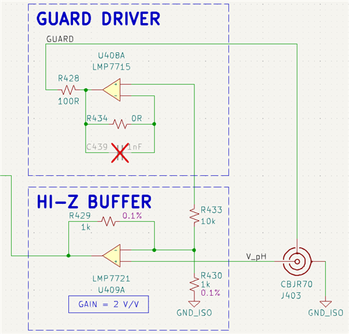
I am using LMP7721 in a non-inverting amplifier configuration with a triaxial connector, as well as LMP7715 to create a guard ring. The triaxial guard and PCB guard are driven to the same potential as the high impedance measurement node (triaxial force / LM7721 non-inverting input). The circuit input is from a very high impedance pH sensor.
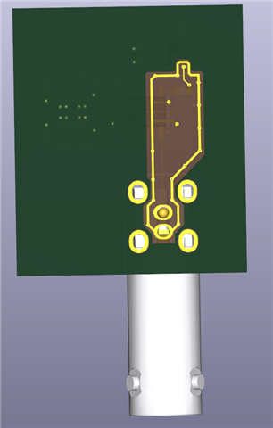
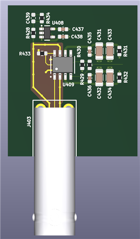
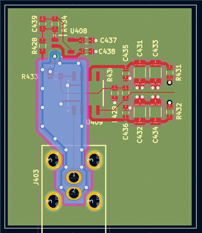
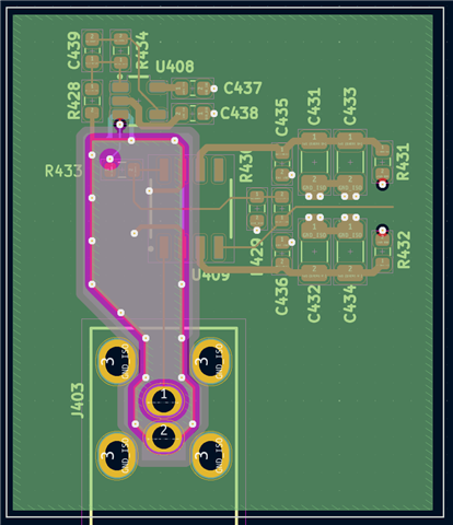
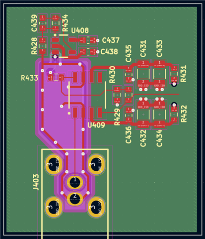
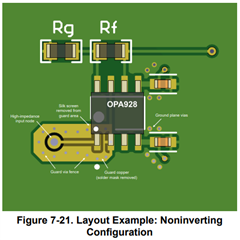
I have done a preliminary layout based on the LMP7721 EVAL board, where the guard trace wraps around both the inverting and non-inverting input of LMP7721, as per both the evaluation board layout and the datasheet. I've noticed however that, in my instance, I could just wrap a complete guard loop around only the non-inverting input (triaxial force). Is there any benefit to doing this, and if so, should I keep the existing extra guard trace that wraps around (but not totally encompasses) the inverting input too?
On another note, this board will be four layers, so on inner layers 1 and 2 I have placed polygons that sits underneath the guarded area of the board, and are also connected to the guard net by regularly spaced vias.
I've attached some snippets of the layout and schematic, with the rest of the design excluded for NDA reasons. In my EDA tool, red is copper on the top layer, and green is inner layer 1. The purple region is a soldermask keepout on top layer. There is a matching soldermask keepout on bottom layer which is easier seen in the 3D screenshot. Blue is tracking on bottom layer.
Any advice / feedback would be greatly appreciated.
Thanks.
