This thread has been locked.

If you have a related question, please click the "Ask a related question" button in the top right corner. The newly created question will be automatically linked to this question.

THP210: Fully Differential Low pass Filter CMRR

Part Number: THP210
Other Parts Discussed in Thread: OPA392, INA592, OPA2392, OPA388

Tool/software:

Dear All,

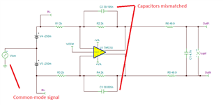
I am designing a fully differential first order low pass filter as part of an ADC drive signal chain. I want to use the THP210 and have my low pass 3db cut at ~2khz.
Design is as below (thanks to EDN for the sketch!)

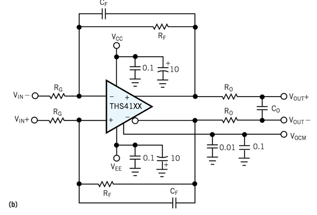
I have VCC=5V, VEE=0, VCM=2.5V.
RG=RF=2k (using a Vishay Dale 4 resistor array with 0.01% matching ratios)
Cf=39nF NP0 1% tolerance. 
R0=49.9 and C0=4.7n.
After R0 is ADC differential.

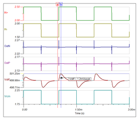
Finally, my input signals are offset square waves (in-phase) on both input pins, with the square wave frequency 1khz.
I.e. for 500us I would have VIn+=2V and VIn-=1.5V, then for 500us I would have VIn+=2.5V and VIn-=2V, and repeat. Obviously I want my output signal to be the difference between the two signals (i.e. in this case one output should be at VCM+0.5/2=2.75 and the other at VCM-0.5/2=2.25V. The overal purpose of my circuit is to measure changes in this difference (which are very slow, <10hz). I will run a SINC filter on the ADC with a frequency cut around 20hz (i.e. rather than doing more aggressive low pass filtering in this analog input part, as my impression was it would require large resistor values that would add significant noise to my signal...).

Now to my question;  I believe I am doing the right thing in my calculation of Cf to give the 2khz low pass, however, does adding this capacitor also dramatically mess with the CMRR of the design - which in this case would lead to 1khz transients turning up in my outputs? If yes, my impression was it wouldnt necessarily matter because differential ADCs are typically giving >>100db CMRR - or is this a datasheet "truth" and in practice my circuit will suffer due to this extra noise injection?


I recognise this is potentially a trivial question but could not find a particularly nice explanation anywhere online...

Many thanks for advice.

  • In case it isn't clear - the purpose of this LPF is antialiasing on the ADC input to avoid adding extra noise from modulation frequency (and harmonics) bands...

    Further, another approach I considered, instead of the above, was sending this signal into an instrumetation amplifier with integrated gain resistors (e.g. INA592 - I don't mind if it gives a 2x gain) to created a single-ended signal, then sending this into an active low pass filter (e.g. sallen key with OPA392 and same cutoff at 2khz) and then through the R0/C0 filter into the ADC. (with the other end of the signal being ground or some other >0 voltage connected to the INA592 reference pin). 
    The downside of this approach is I think it would give greater offset error/drift than the differential mode approach described above, but perhaps it solves some of these CMRR problems. My overall impression was that if using a differential ADC it was sensible to get your signal path differential as soon as possible, hence my questions above.

    As described above the overall goal is to get best possible DC/low frequency drift/offset/noise performance. These are the considerations I am trying to weigh in decision. 

  • HI H S1,

    If the input signal has a square wave in-phase on both input pins, with the square wave frequency 1khz, and VIn+=2V and VIn-=1.5V, for 500us and VIn+=2.5V and VIn-=2V, then in this case, you are injecting a 1kHz, 250mVpk common-mode square waveform signal.  As you have mentioned, the square waveform will have higher frequency odd harmonics.

    As you have explained on the post filter above, the THP210 circuit with the 39nF feedback capacitors and RG=RF=2k has a cutoff corner frequency around 2kHz. The THP210 / filter helps rejecting/attenuating the high-frequency common-mode content of the 1kHz common-mode signal.  Although you are using ±1% C0G capacitors, the mismatch of the feedback capacitors provides a rejection degradation at the low frequencies. For example, purposely mismatching the feedback capacitors by ±0.5%, and injecting the common-mode signal you describe above, produces a differential residual noise of 1.2mVpeak with a fundamental around 1kHz.

    - If you are interested only on a DC measurement, is it possible to apply a lower frequency input common-mode filter with a corner frequency at a few 10s of Hz?  This will help attenuate the1kHz fundamental common-mode signal prior it reaches the circuit.  For example, using a passive RC low-pass filter with a lower corner frequency around ~40-Hz, with a OPA2392 buffer amplifier stage, followed by the THP210 attenuates the noise considerably before reaching the ADC at around 240uV peak. I assumed using precision resistors and 1% 100nF C0G capacitors at the inputs.  Using a lower-corner on the input filter helps reduce the 1kHz ±250mVp common-mode signal to ±40uV.  The ADC SINC filter at ~20Hz should help provide additional attenuation of this 1kHz differential noise signal..  This circuit provides a low offset and low drift error assuming precision resistors are used.

    There are other alternatives such as implementing a Sallen-Key filter on the OPA2392 stage providing further attenuation, but requiring more passive components.  The corner of the low-pass filters needs to be set at a frequency well below the 1kHz common-mode signal to help eliminate the fundamental.

    Thank you and Regards,

    Luis


  • Thanks Luis, that's really helpful.
    There are three things I am still not quite clear on:

    1. If my SINC filter in the ADC has >100db rejection at the 1khz frequency, why bother with the extra LPF? Should I not believe the ADC will do as expected in practice? I had assumed I might have (for example) the 1.2mVpp 1khz residual (as you suggested) going into the ADC, but that with 100db rejection by SINC filter at this frequency, the 1khz signal would be <1uVpp and hence below ADC noise/1LSB.

    2. Perhaps counter intuitive, but by increasing the THP210 low pass filter cutoff could we improve this component-dependent mismatch? I could probably put this up to 10k cut frequency (I need to attenuate at least 10db at 60khz to avoid any significant aliasing so have flexibility here), which would reduce its impact at 1khz and the next few harmonics and thus (somewhat) limit the impact of filter mismatch. Then, I also thought the opposite of this might be viable - for example increase Cf in the design (e.g. to 0.1uF or 0.22uF which I can get in 1206 NP0 packages) to further reduce the cut frequency well below the 1khz. This would slow down the output significantly, but since my input signal doesn't change too fast I don't think this would cause issues with ADC driving (since the kickback filter only has to settle the kickback rather than some major signal change with each sample). 

    3. The second solution I suggested (in my initial reply to my own post) could do as you suggest (add an extra LPF) with fewer components (i.e. just 2 Opamps and fewer discrete components). But, does going for a single-ended solution lead to other issues down the line? 

  • Hi H S1,

    It is difficult to comment in detail on your ADC driving requirements, the digital filter rejection, and anti-aliasing concerns, since there is no ADC information on the post above.

    The analog filter design depends heavily on the ADC spec and the modulator frequency, assuming this is a delta-sigma ADC. The modulator frequency, can be anywhere as low as a few 10's to 100's of kHz for some ADCs used for DC measurements. Aliasing could start to become a problem for these ADCs using low modulator frequencies, if you were to relax the analog corner filter to 60-kHz. Nevertheless, on other higher bandwidth ADCs, the modulator frequency can be set at a much higher frequency, at around the the ~10s of MHz range, which will allow you to relax considerably the analog filter corner frequency requirement.  

    In some cases the SINC1 filter should be enough to allow you to reduce the noise, assuming the modulator frequency is set several decades higher compared to your analog filter cutoff frequency. Assuming that the modulator frequency is set at several decades higher than the analog filter, the SINC filter should offer high rejection at multiples of the sampling frequency. This "ideally" will reject a lot of the noise, as you mention at 100dB rejection at 1kHz. 

    The potential issue for aliasing on a SINC filter for a Delta-Sigma ADC occurs when the noise signal frequency occurs close to the modulator frequency, or close to multiples of the modulator frequency.  For example, on the normalized plot below, the rejection of the SINC filter, at frequencies above >0.5 modulator frequency, shows that the SINC filter rejection degrades, where the SINC filter offers no attenuation at the multiples of the modulator frequency. See the normalized fin/fmod plot below for an example of a digital SINC filter. 

    Nevertheless, using a passive low-pass filter in the analog domain reducing the 250mV peak signal will help reduce the risk of coupling high-frequency harmonics AC signals into your sensitive analog inputs. The corner frequency of the analog filter needs to be set to provide enough attenuation at frequencies close to the modulator frequency where the ADC digital filter rejection degrades.

    Many modern fully-differential ADCs can be used on single-ended fashion and still provide very good performance.

    The ADC sampling structure, the availability of pre-charge buffers, or whether this ADC incorporates an amplifier front-end can make a difference in providing a detailed answer. If you wish us to provide suggestions, please provide the ADC details, such as modulator frequency you wish to operate, whether this is a simple first order SINC filter or higher order, etc.  If device part number, or data sheet is available, kindly provide. 

    Thank you and Regards,

    Luis    

  • Thank you. I have had a look at this; we are using AD7768 as we need to have 8 fully independent channels (i.e. no mux) to read out from many such inputs at once. We've gone through the datasheet and it seems that indeed we can have our fmod down to about ~70khz and so adding extra filtering is wise.

    I have also then done a series of simulations in TINA with similar schematics to what you suggested above (i.e. THP210 and active filters added). I went to OPA388 for lower drift than OPA392.

    This left one final (hopefully) question. In your simulation above you put the low pass filters upstreamof the THP210. However, in simulating this it is seems clear that component value mismatch on either the RC filters or THP210 would couple in 1khz to the differential mode (as you discussed before). However, if you put the low pass filters/buffers downstream of the THP210 then component errors on the RC filters have no impact on rejection of 1khz. 
    Therefore, I wondered why your schematic (and indeed the vast majority in datasheets for ADC drivers) do the RC filters upstream? My intuition is that it is because in most cases people are interested in fairly fast signals and hence need a strong buffer for the ADC input kickback filter, whereas our small fmod=60khz (and the ADC's input buffers + SINC4 filter which will have -3db cut around 20hz) signficantly reduces this requirement.

  • Hi H S1,

    In conventional/generic applications, the noise at low frequencies is primarily due to the 50/60Hz line noise and a few low amplitude 50/60Hz frequency harmonics typically limited to less than 3kHz that are normally rejected by the SINC filter alone, and there is no other dominant noise components. Hence on most conventional applications, a simple R-C filter suffices. This application has the 1-kHz square common-mode signal, so the concern is primarily the high frequency odd harmonics. 

    You are correct, I responded to the original question with a conservative, very low corner frequency filter at the THP210 without altering the ADC input kickback filter because I did not have immediate information on the ADC drive requirements, nor the digital filter rejection and modulator specs available. Although there was a low level differential residue noise due to component mismatch on the original response above, this residue was still small. However, in this case, since this is a Delta-Sigma for DC measurements that includes pre-charge buffers, there is flexibility on altering the ADC input filter as well.

    Let me know if you need us to verify the circuit for stability.

    Thank you and Regards,

    Luis