This thread has been locked.

If you have a related question, please click the "Ask a related question" button in the top right corner. The newly created question will be automatically linked to this question.

INA122: INA122 - Non Linear Output with a positive and negative input

Part Number: INA122

Tool/software:

I intend to measure the difference in voltage using the INA122 and generate an output with an offset of 1.425V running on a +2.85V supply.

With no input or 0V between J7 and J8, the output of the IA is 1.426V

With a voltage input of 20V(J8-J7), the voltage output at the IA is 2.344V

With a negative input of 20V(J8-J7), the voltage output of the IA is 0.478V

Checking the difference between the positive and negative input with reference to the output when there is 0V applied, there is a 30mV difference. 

Hence, there seems to be a non-linearity when measuring a positive and negative input voltage.

The circuit diagram and the table shows the details of the above mentioned.

I would hence like to seek any advice on the possible issue and how the issue can be resolved.
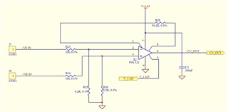
       

INA 122
VIN + - REF CV+OUT
J8 - J7 X2 P3 X2 P2 X2 P5  X2 P6
-20.05 -0.0618 0.0618 1.425 0.478
0 0.0000 0.0000 1.425 1.426 0.948
20.05 0.0618 -0.0618 1.425 2.344 0.918
  • T W,

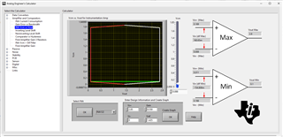
    I think the issue you are seeing is common mode range limitation.  The INA122 and other similar devices have a valid common mode range that is related to the power supplies.  For instrumentation amplifiers the common mode relationship can be somewhat complex.  It depends on the gain, volage reference pin, and supply voltages.  The best way to understand the common mode range is with Vcm-vs-Vout plots (sometimes called diamond plots).  The data sheets for instrumentation amplifiers will normally show a few diamond plots, but often the plots in the data sheet do not cover the particular set of conditions that you require.  The ANALOG-ENGINEER-CALC has a INA Vcm vs Vout tool where you can enter your conditions (see image below for your case). 

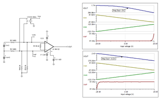
    Vcm is calculated as the average voltage applied to both inputs: Vcm = (VinP + VinN)/2.  In your design the common mode will range from -61mV to +61mV.  The negative supply in your design is GND.  The INA will not allow Vcm all the way to GND.  Looking at the Vcm plot you can see the common mode is limited to about 0.088V from GND.  This issue could be solved by using a negative supply or shifting the common mode on the input signal.  The simulation below shows your circuit with a 0V negative supply and a -0.2V negative supply.  The case with the 0V supply is non-linear because the Vcm range is violated and the case with the -0.2V supply is linear(see simulation below).

    I hope this helps.  Let me know if you have follow up questions.

    Best regards, Art

  • Good day Art,

    Thank you for your detailed explanation on the common mode range limitation that I have with the design.

    I will have to study futher to see if there is other means to not violate the Vcm range.

    Thank you for your advice once again.

  • Good day Art,

    After changing the common mode voltage at the input from GND to VREF=1.425V, the output voltage non linearity issue is resolved.

    INA 122UA
    VIN + - REF CV+OUT
    J8 - J7 X2 P3 X2 P2 X2 P5  X2 P6
    -20 1.3630 1.4860 1.425 0.511
    0 1.4250 1.4250 1.425 1.426 0.915
    20 1.4860 1.3630 1.425 2.342 0.916

    Thank you very much for the advice.

    Have a great day.