This thread has been locked.

If you have a related question, please click the "Ask a related question" button in the top right corner. The newly created question will be automatically linked to this question.

OPA855: I have a dc bias problem when use opa855 as C-TIA

Part Number: OPA855
Other Parts Discussed in Thread: OPA277, OPA858, OPA657

Tool/software:

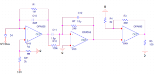
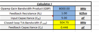
I'm currently testing a C-TIA circuit using the OPA855.

I'm experiencing a DC bias issue in my test setup. The non-inverting input of the OPA855 has a bias of 3.8V, while the inverting input has a bias of 3.2V.

I believe this 0.6V difference in input bias is causing the OPA855 to saturate. However, the OPA855's output has a DC bias level of 3.4V.

Can anyone explain why this situation is occurring and provide guidance on how to achieve the desired 3.8V output DC bias level?

I'm using an OPA277 to generate a 3.8V DC bias voltage in my circuit.

  • Hello Shin,

      Would you be able to try testing with a smaller feedback resistor, and rely on the second stage for the additional gain, or is your input current too small? The reason why is because of the bipolar architecture of the OPA855 means it will have a higher bias current which causes an additional offset voltage at the output.

      If you do not need the very high bandwidth, you could also replace the OPA855 with the OPA858 which is a FET input 5.5 GHz amplifier. As a CMOS/FET input voltage feedback amplifier, it naturally has very low input bias current. 


    Thank you,

    Sima 

  • J.-H. Noh, “Frequency-Response Analysis and Design Rules for Capacitive Feedback Transimpedance Amplifier,” IEEE Transactions on Instrumentation and Measurement, vol. 69, no. 12, pp. 9408–9416, Dec. 2020, doi: https://doi.org/10.1109/tim.2020.3006325.
    I referenced the above paper for the TIA configuration. I conducted tests using a 2k ohm resistor for R1. In this setup, I observed that both the input and output terminals have the same DC bias of 3.8V. 
    In this setup, the TIA is functioning as a resistive TIA rather than a capacitive TIA.
    I need a bandwidth of 350MHz. Would the OPA858 be suitable for this?

  • Hello Shin,

      Thank you for sharing the reference and trying out the suggestion. Just to confirm, did the change give you the correct values that you expected?

      It depends on your input capacitance from your diode and the minimum gain you need to observe the signal at the output of the first stage. With 1Mohm feedback resistor, the OPA855 would not be able to achieve 350MHz. Therefore, it is possible to keep the OPA855 if you are able to decrease the gain on the first stage.

      Overall, my questions are:

    1. Did the suggestion of decreasing the feedback resistor, R1,  give you the correct value that you were expecting?
    2. What is your photodiode's capacitance
    3. What is your photodiodes output current range (min to max amp value)

    Thank you,

    Sima

  • According to the reference, the bandwidth can be expanded through the use of a differentiator in the second stage, allowing you to achieve the desired bandwidth.

    1. When I used 2k ohms for R1, I obtained the expected results.

    2. I am using the MTAPD-07-013, which has a capacitance of 1.2 pF.

    3. 1uA - 10mA range

  • Hello Shin,

      Thank you for the additional information.

      I went through the reference up until the DC servo loop section, and it is very interesting I see what you mean between CF-TIA vs RF-TIA.

      The max gain is both first and second stage from reference:

      vs in RF-TIA

       However, based on this statement, the gain is indeed the combination of the two stages. And, you are correct that the bandwidth extension is due to the second stage. The addition of Cd or C11 in your schematic changes the placement of the poles/zeros which affects the crossover of the noise gain and AOL to be further in frequency. 

       In comparison, here is the crossover for RF-TIA:


       With your input current range, you might benefit from a different structure. You may keep the OPA855, but then follow this with a variable or programmable gain amplifier. Because, for example, if you have a high gain for your min current then you will saturate the amplifier at your max current. 

       Therefore, for first stage:

       Then second stage would be another amplifier with internal gain switches such as our VGA/PGA which would be useful also if you are following this up with an ADC. 

        If you do need high gain for a different input current range or this project is for research purpose on CF-TIAs, then the OPA855 can be replaced with the OPA858 since it is a p2p (pin to pin) which makes it easy to replace on the same PCB board. And, you may be eligible to order a sample via the ordering & quality tab of the device:

       The DC issue would go away because of CMOS architecture, also referenced in J.-H. Noh's paper "The CF-TIA was initially proposed for reducing the thermal noise generated by the RF-TIA’s feedback resistor and for overcoming the difficulty in integrating a high resistance in the CMOS chips" and uses the FET-input OPA657 as the example device. 

    Best Regards,

    Sima 

  • I am planning to use an AGC structure after the TIA.

    But, The noise of the TIA limits the system's dynamic range due to its impact on the signal-to-noise ratio (SNR).

    So, I am conducting research on low-noise and low-gain TIAs implemented in CMOS technology to prevent amplifier saturation.

    I have OPA858 too, i'll replace OPA855 to OPA858.

    Thank you