This thread has been locked.

If you have a related question, please click the "Ask a related question" button in the top right corner. The newly created question will be automatically linked to this question.

INA296A: Noisy amplifier output

Part Number: INA296A

Tool/software:


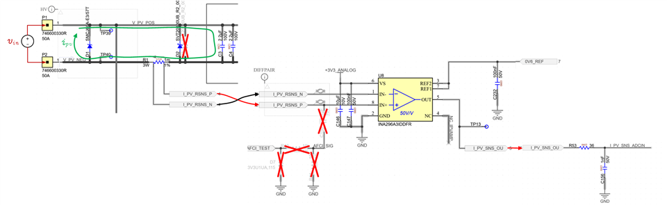
The above is an implementation for low-side current sensing based on INA296A3IDDFR in my project. Whilst validating the circuit, I found that the output at I_PV_SNS_OU with respect to GND is quite noisy. Here is a waveform captured when the current flowing through sense resistor R1 is about 50mA

Observing this, I proceeded to measure 0V6_REF and 3V3_ANALOG, both with respect to GND and did not observe the same noise pattern  

Other things we have tried include:

1. Replacing R53 with 360Ω (to decouple the 1nF capacitive load from the amplifier based on INA296A: Floating noise much higher than spec - Amplifiers forum - Amplifiers - TI E2E support forums)

2. Replacing C156 with a 270pF capacitor (since 1nF is exactly equal to the maximum tolerable capacitance for this component)

3. Removing R53 altogether and measuring the output at I_PV_SNS_OU (No capacitive load on the output)

None of these actions had a noticeable effect on the output waveform and we continued to observe the same noise pattern and I am wondering what other actions I could take to reduce this noise?

Would appreciate any recommendations.

  • Hafis,

    Thank you for your patience. Due to the U.S. holiday, the team is out of the office, but will reply when we return on Tuesday, 1/21.

    Louis

  • Hafis, 

    Based on such a small current and shunt, the output you are seeing here is simply the noise of the device, at full bandwidth referred to the output. From the datasheet, we can grab the noise density spec and curve over frequency:

    The total noise output would be the sum of integral under the curve for figure 6-27. Granted, this is a loose approximation, but if I run a simple brick wall analysis for the G=50 V/V variant, I would get

    RTI noise, RMS = 39NV/sqrt(Hz) * sqrt(1.1MHz) = 40.9uVrms. 

    Converting this to peak to peak, and pushing through to the output, 

    40.9uVrms * 6.6 * 50V/V = ~13.5mVpp

    Based on the scope shot you show, I would say you are seeing ~10-12mVpp on the output, which aligns with this calculation (since I am overestimating with the brick wall simplification). 

    So, if it is indeed the inherent noise of the part, there are few ways you could tackle this: you could throttle the bandwidth on either side of the part via low pass filter (be careful to not inject error into your signal chain on the input side), or you could select a higher gain device as per figure 6-27 to reduce the noise on your signal chain. 

    Some notes on what you have tried:

    1. Replacing R53 with 360Ω (to decouple the 1nF capacitive load from the amplifier based on INA296A: Floating noise much higher than spec - Amplifiers forum - Amplifiers - TI E2E support forums)

    - In this case, the output filter you created limited the bandwidth on the output side of the filter to ~440kHz. This should reduce noise beyond the filter to about 8.5mVpp by the same analysis above. This is quite a small adjustment, so it is possible it did not seem like an improvement. The current filter shown in the schematic limits to 3MHz, so I would not expect much filtering from this. 

    2. Replacing C156 with a 270pF capacitor (since 1nF is exactly equal to the maximum tolerable capacitance for this component)

    This limited bandwidth to 11.1MHz, so apart from light HF noise, I would not expect to see any improvement here. 

    3. Removing R53 altogether and measuring the output at I_PV_SNS_OU (No capacitive load on the output)

    - Since I believe this to be the noise of the part, I do not believe it is the filter causing this. 

  • Hi Carolus,

    Thank you for the analysis and response.

    I had come to a similar resolution of filtering the signal, but was baffled by the source of the noise.

    I have found that the noise largely cancels to zero with more vigorous filtering on the output and would like to apply this solution.

    I was further wondering if there could be any conditions where filtering the noise could introduce offsets in the output signal?

    Thanks 

  • Hafis, 

    The only offset I can foresee would be the due to the sizing of the resistor. As you increase the resistor size, the offset between the pin, ie, the true response of the part, and the DC value on the opposing end of the filter will deviate. Of course, reducing the resistor (and increasing the capacitor to maintain the same cutoff frequency) runs you into damping issues as the phase margin goes down on capacitor increase. I would say try a few differing values of RC to achieve the desired cutoff frequency you would like and look at a step response to see what kind response you have. A small amount of overshoot should be ok here.