Other Parts Discussed in Thread: AMC0381D-Q1
Tool/software:
1 . In the layout guidelines of AMC0381D-Q1 , there is nothing mentioned related to inner layers and bottom layer placement and routing.
We are using this IC in our 6-layer board and would like to know the guidelines for routing VDD1 and GND1 planes in inner layer under this IC. Also is there any placement restrictions on bottom side for other components , if this IC is placed on TOP layer?
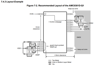
2. As per layout guideline >9.2 mm creepage is required between HVIN pin and VDD2 Pin .
Actual distance between these two pins is approx. 8.232mm. If we add slot on PCB this will increase creepage distance on PCB, but IC itself has lower creepage than 9.2mm. Please guide how to achieve this creepage requirement.