This thread has been locked.

If you have a related question, please click the "Ask a related question" button in the top right corner. The newly created question will be automatically linked to this question.

VCA824: Fully differential summing amplifier

Part Number: VCA824
Other Parts Discussed in Thread: LMH6554, TINA-TI

Tool/software:

Hello,

I designed a fully differential summing amplifier using the VCA824. Based on the values of Rg and Rf, I expect a gain of 5. However, the simulation results differ from this expectation.

Could you please check where I might have made an error?

Thank you for your assistance.

Diff-In_Sum-VCA824.TSC

  • Hello Mojtaba,

    I am working with your TINA schematic and simulation.  Could you confirm your input voltages and desired output voltage levels?

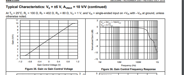
    I did find a curve for Av_max = 10V/V where a Vg = 0 setting results in Av = 5 V/V:

    You should try Rf = 402 Ohms; the Rf in a VGA product (variable gain amplifier) is not directly setting the signal gain; the Rf and Rg only set the maximum gain.  You can choose to set the maximum gain to 5V/V if you would like, otherwise you can use the Av_max = 10V/V example and set Vg to zero.

    I will look into the simulation once you provide your target input and output values.

    Best,

    Alec

  • Hello Alec,

    Thank you for your reply.

    I set the Vg = 1, Rf=200 and Rg=80 to achieve Av = Av_max = 5 V/V. My goal is to design a fully differential summing amplifier, where two inputs are differential signals from twisted pair cables with 100-Ohm impedance. However I am unsure why the result shows an approximate gain of 2.5V/V instead of the expected 5V/V.

    I would appreciate any insight you may have.

  • Hello Mojtaba,

    When performing a transient simulation I observe output swing peak-to-peak of 1.44V, which is a gain of ~4.8V/V to your combined 300mVpk-pk input signal.

    Do you have a target output voltage value you need to drive the subsequent circuit?

    I see you are summing a 50mV sine wave with a 100mV sine wave from your twisted pair cable inputs; this results in a 150mV amplitude sine wave at the VGA.

    You should be expecting ~750mV amplitude on the sine wave at the output, with a Vpk-pk = 1.5V.  

    While the existing simulation is not exactly what you defined, the output is behaving closer to 5V/V of gain than you originally observed.

    Diff-In_Sum-VCA824_TI.TSC

    Best,

    Alec

  • Hi Alec,

    Thank you for reviewing the simulation file.

    I noticed that you changed the Rf value to 402 Ω to achieve a gain of 5 V/V. However, based on the datasheet, the gain should be approximately 2 × (Rf / Rg), which in this case results in 10 V/V. Is there something I might be overlooking?

    This gain will eventually be controlled by the output of another stage, but for now, I am struggling to properly set the gain for the summing of two differential inputs.

    I would greatly appreciate any insights you may have.

    Regards

  • Hello Mojtaba,

    Your understanding is correct; I had set the name of the resistor to 200 Ohms instead of the value of the resistor.  The maximum gain is set by 2 x (Rf / Rg); when you use Rf = 200 Ohms and Rg = 80 Ohms, the maximum gain is set to 5V/V.  With VG = 0 to observe ~ 2.5V/V gain, and with VG = 1V I observe ~5V/V gain.

    The difference between ideal and simulated values may be due to the gain error and limitations of the design of the VCA82x devices.

    Best,

    Alec

  • Hello Alec,

    I tried using LMH6554 for adder stage and integrated it with the VCA824 to provide gain control. However, it seems that the VCA824 does not support differential input, so only out+ of the LMH6554 is connected to it, which has a DC offset. when I place a capacitor to block the DC, the total output drops significantly.

    Could you please check where I might have made an error?

    Regrads

    Diff-In_Sum-LMH6554_VCA824.TSC

  • Hello Mojtaba,

    Yes, I can check on this design for you.  Allow me time now and on Monday to investigate.

    Best,

    Alec

  • Hello Mojtaba,

    Please see the attached TINA-TI file.  

    I have a few points for you that I learned through simulation:

    1. You need to account for proper input termination and differential drive of LMH6554.  In the simulation circuit, I used single-ended inputs for simplicity and followed the datasheet guidelines on page 15 for input termination.  On your original schematic, input termination was just 50-Ohms without any correct setting of Rg resistors and termination resistors.  

    2. If properly 50-Ohm matched at the input, the circuit will experience 1/2 attenuation due to this match in simulation.  I use the LMH6554 in 2V/V (6dB) gain to accommodate this behavior.

    3. The inputs to VCA824 require resistive path to ground after DC blocking capacitors, these resistors allow for proper resetting of the common mode input voltage and present the 200mVpk-pk signal at the VCA inputs (differentially).

    4. Setting VG=0V on a 10V/V Avmax setup results in 5V/V gain, with a 500mVpk-pk Vout.  This shows system viability for your design.

    differential_adder_full_signal_chain.TSC

    Best,

    Alec