This thread has been locked.

If you have a related question, please click the "Ask a related question" button in the top right corner. The newly created question will be automatically linked to this question.

INA326: RTD connection with REF200

Part Number: INA326
Other Parts Discussed in Thread: REF200

Tool/software:

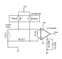
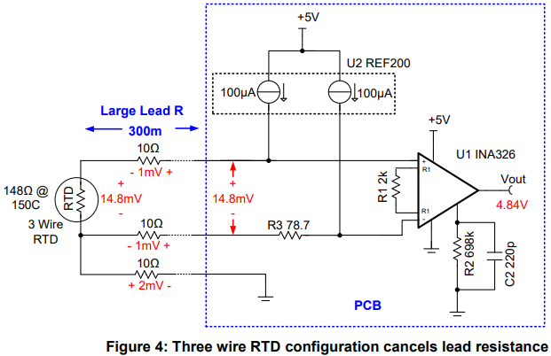
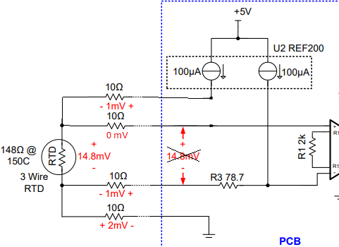
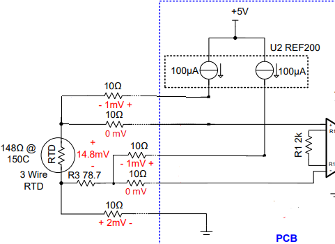
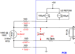
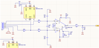
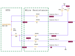
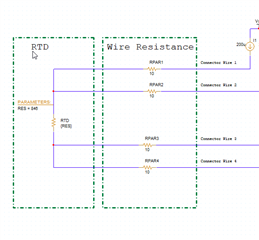
In the document “RTD to Voltage Reference Design Using Instrumentation Amplifier and Current Reference”, the above 3-wire PT1000 connection is made.

How can I make a 4-wire PT1000 connection with the same component (Ref200 and Ina326) and the same design?

  • The 3-wire design relies on the resistance of the wires being the same to cancel out the voltage drop over the wire resistance:

    In general, a 4-wire design uses two wires with a current of nearly zero so that there is no voltage drop over the wire resistance. However, with R3 and the additional current through it, there is a voltage drop in the third cable, so now the measured voltage includes the cable's voltage drop. So this design is worse than the 3-wire design; you have to either calibrate out the actual cable used, or remove R3 and the second current source and adjust the gain and offset accordingly (see figure 6 of the INA326 datasheet).

    To ensure that the current through R3 does not result in a voltage drop that is included in the measurement, you have to move R3 to the sensor and use a 5-wire design (but then R3 is also affected by the temperature to be measured):

  • Hey Clemens,

    Wouldn't it be sufficient to use the INA326 in the below configuration? Is that what you are describing in the second paragraph? This doesn't utilize the two current sources of the REF200, so a single current ref is all that is needed, but then there is no need to compensate for lead resistance. Additionally, the gain setting resistors will have to be adjusted for the acceptable input range and input differential range of the INA326.

    The drawback here is that the input voltage does not get as low for the minimum resistance, but the gain setting resistors can be adjusted accordingly to have a valid output range and maximize the output scale range.

    Best,
    Gerasimos

  • Yes; this measures the total voltage over the RTD, so the usable range at the amplifier is smaller.

  • Will it work if I make the design this way? The range I want to measure, that is, Tout should be 0 V at -40 degrees and 3.3V at 85 degrees. Can I achieve this in this design?

    One leg of the RTD should enter the 1st and 2nd inputs of P10 and the other legs should enter the 3rd and 4th legs.

    Are there any calculations such as the calculations in the “RTD to Voltage Reference Design Using Instrumentation Amplifier and Current Reference” document for this design? For example, how can I calculate the voltage output at 25 degrees?

  • Hey Gulbahar,

    To accurately answer this, I will need to know what value of RTD you are using, and what the nominal value is (usually specified at 0C). Providing the datasheet of the RTD will let us accurately calculate your range of voltages over your temperature span.

    Please note that the output of the INA326 cannot swing all the way down to 0V. I would limit the lower end of the targeted output voltage to 0.1V or 100mV.

    Best,
    Gerasimos

  • Hello Gerasimos,

    https://www.mouser.com.tr/ProductDetail/YAGEO-Nexensos/32208572?qs=MQgg6%252BVqoaMqkqBu%252BAlGZg%3D%3D&srsltid=AfmBOorj_fNBEbBKyb4Q-clPBkfCriwd6DA8E9NdQ2fMGdvJJzddRl9g

    This is the RTD resistor we use.

    These are the nominal resistance values.

    As output voltage, output voltage to 0.1V or 100mV is suitable for me.

    Thank you.

  • Hey Gulbahar,

    If you are trying to replicate the same compensation with a 5 wire setup for the RTD, the implementation would look like the following, which lines up with Clemens' setup:

    When implementing this, you ensure that you will see an equal but opposite voltage drop due to wire parasitics on both inputs. However, the notable drawback here is that the R1 compensation resistor must be local to the RTD, and will be exposed to the same temperature stresses as the RTD, with notably less linearity in resistance shift over temp.

    Connecting the circuit as below eliminates parasitic resistance drop over the wires, but does not allow for the R1 compensation to establish a smaller Vmin.

    If you are trying to implement this compensation scheme, I would recommend following the three wire method. If you are making the RTD and have control over how many wires you want the RTD to be, you can choose to make this a three wire design and follow the methodology outlined in the app note. I do not see a benefit of increasing the number of wires in the RTD implementation. Is there a specific purpose you wanted to use a 4 wire topology?

    Best,
    Gerasimos

  • Hello Gerasimos,

    I made this design. I calculated output voltage for this design. -40 degrees 0.2 V and 80 degrees 3.2V. and I think results sutitable for me.

    I want to 4 wire RTD design because I used this interface design for sensor. Sensors are commucation far distance and sensitive measure. So, I used 4 wire commucation, instead of 3 wire. 

    İs it true this design, Am I right. 

    If you have any improvements about this design, can you share it with me?

    Thank you for your interest.

  • Hello Gulbahar,

    This will only give you the correct calculated output if there is no parasitic resistance. However, you intend to run a long cable to run this measurement. Once these parasitic resistances are added, there will be error.

    Connect VIN+ and I2L to pin 1 of RTD, leave pin 2 floating.

    Connect pin 3 of RTD to one side of 835 ohm resistor.

    Connect other end of 835 ohm resistor to I1L and VIN-.

    Connect Pin 4 to GND.

    I'm assuming earth GND is separate from the RTD GND.

    This method will compensate for parasitic wire resistance similar to https://www.ti.com/lit/ug/tidu969/tidu969.pdf

    Best,
    Gerasimos

  • Hello Gerasimos,

    Thank you for all your guidance.