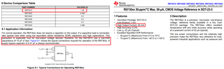
This thread has been locked.

If you have a related question, please click the "Ask a related question" button in the top right corner. The newly created question will be automatically linked to this question.

TL074: Remove the voltage follower function

Part Number: TL074

Tool/software:

Hi TI experts,

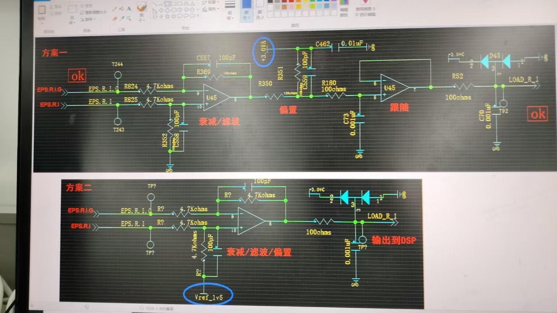
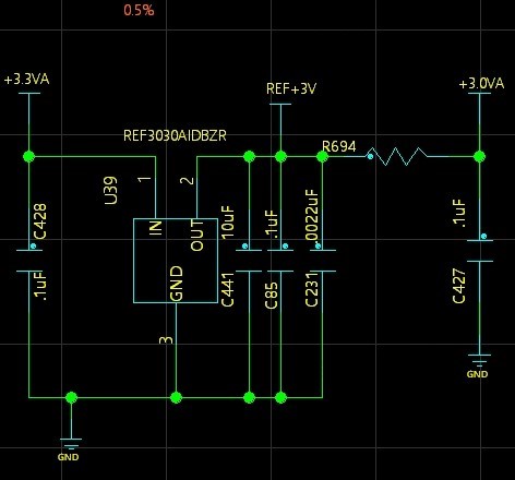
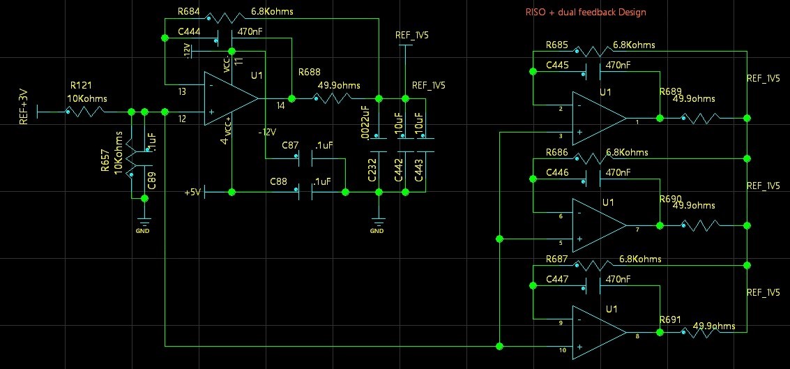
My customer used to use TL074 for much channels current and voltage sensing in solar inverter project.

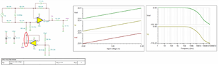
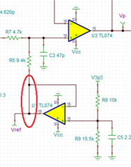
They use two channels of TL074 for one signal sampling. One for Due to they have two much signals need to measure. So they changed the offset setting and move it before the first amp channel, which can save the second amp channel.

Question: Do they still need voltage follower in bottom schematic?

  • The first schematic has two R-C LPF filters, before and after the buffer. The second schematic has only one. If this is OK for your signal, then the second schematic will work.

  • Hi Gary, 

    I agreed with Clemens. If the 2nd one works for your application, use the 2nd one. 

    Here is an alternative suggestion. Since I do not have your design requirement, I am proposing the alternative example.

    The differential Vsense for current sense input is incorporated with a differential LPF. The input impedance should be matched to +/-1% or better, and and Vref needs to be an low impedance node for a difference amplifier. The Vref is required to have source/sink capable node to have a fast response at Vp and Vout. 

    Since this is solar inverter current sense application, the circuit may be able to further limiting the BW and remove any possible high frequency noise (lower the differential and common mode passive LPFs). 

    TL074H DA Isense 04172025.TSC

    If you have other questions, please let us know. 

    Best,

    Raymond

  • Hi Raymond,

    It seems that you also add a amplifier as voltage follower for 2V offset. Does Vref node need capacitor?Customer has so many current sampling channels, up to 40x, can they use same 2V offset from one amplifier.

  • Hi Gary, 

    It seems that you also add a amplifier as voltage follower for 2V offset. Does Vref node need capacitor?

    TL074H is required to have Vcm_min = 1.5Vdc, and I set the Vref pin to 2Vdc to increase the design margin.  

    For 40X channels, you need only a handful of Vref circuit near the location of difference amplifiers, say four of Vref circuits - one Vref for every 10 difference amplifiers or so. The Vref node will not drive much current, but it has to be able to source and sink current if it is required. 

    The Vref circuit needs to be localized, and I do not want that the reference circuit to run all over the PCB layout (because it will pick up unwanted noises). 

    Yes, it needs to have 1uF to 2.2uF capacitor to filter out 3.3Vdc noise, and keep localized to difference amplifiers (keep short traces). 

    sampling channels, up to 40x, can they use same 2V offset from one amplifier.

    Technically, this can be ok. But the PCB traces are too long if it is done for all 40X. It is preferable to be localized and implement short PCB leads. 

    If you have other questions, please let me know. 

    Best,

    Raymond

  • Hi Raymond,

    Customer wants to use dual feedback divide Vref 3V to 1.5V for up to 50ch Vref_1v5 in above first picture. 

    Customer wants to use REF3030 to output 3V and then use 4ch TL074 as 1.5V voltage follower for 50ch amplifiers in above picture1.

    Is this dual feedback architecture feasible?

  • Hi Gary, 

    Customer wants to use REF3030 to output 3V and then use 4ch TL074 as 1.5V voltage follower for 50ch amplifiers in above picture1.

    Please follow the REF30xx datasheet recommendation. Although the REF30xx is able to handle certain large capacitive load, but it is not advised, if the Cload is increased beyond the recommendation.  

    I would recommend to use REF30xx as it (if possible). TL074 is not a precision op amp and the Vref generated from REF30xx may create unwanted offset voltage, and they may not be as consistent as REF30xx bandgap reference. 

    The op amp's dual feedback compensation works, but your circuit seems to drive excessive large capacitive load.  This will significantly reduce the Vref's response (in terms of BW). When op amp drives large capacitive load, it uses its BW to trade of for its op amp stability, so the BW is typically low or very low when driving large capacitive load (e.g. 20uF). Even you follow the follow the dual feedback compensation slide, we have to go through the loop analysis and make sure the op amps are stable. 

    What are the 1.5Vdc references for? What are cost consideration for these reference? Let me see if I can find a better solution to your application. Can the customer use 1.25Vref for your application?

    Best,

    Raymond