This thread has been locked.

If you have a related question, please click the "Ask a related question" button in the top right corner. The newly created question will be automatically linked to this question.

INA326: RTD Example circuit

Part Number: INA326

Tool/software:

We are trying to replicate the operation of the example RTD circuit given in both the REF200AU/2K5 data sheet and application note tidu969.pdf. Our operation in no way resembles the expected results in the data sheet. After running the PSPICE simulation on the circuit, we confirm that the operation doesn't resemble the published circuit. Can you please give us a clue as why this is? Was there an errata that we missed? We have designed a temperature sense system based on these TI parts and are disappointed by this disparity.

  • Hey Russ,

    Could you please expand on the disparity you are seeing? Are you able to share an archive of your simulation? If you would like to avoid posting the archive on the forum, you may message me directly. I have sent you a request to connect.

    Best,
    Gerasimos

  • Thanks for getting back, Gerasimos. I sent you an email with a snip of the schematic as I’ve implemented it. It is an almost exact duplicate of the data sheet’s example (tidu969.pdf).

    Our circuit is outputting a roughly 200mv positive offset and we can’t figure why it’s doing that. Our pspice simulation also generates an inordinate offset (around 50mV with the RTD input shorted) using the TI supplied part models. Can you shed some light on why this is and why the disparity between the application notes (data sheets) and the actual results?

  • Hey Russ,

    I don't believe I received anything in my email. I've sent you a message with my email address.

    Best,
    Gerasimos

  • So doing a little more research on the amp, I'm finding that, according to the data sheet, an offset can be expected up to 100µV. This seems like a lot, especially given the low input diff voltage expected. Something like this should be mentioned in the circuit example. So, if this offset is expected, is it constant between devices, or is a crap shoot? Can it be statically compensated on the output?

  • Hey Russ,

    Correct, with the gain you provided, you can expect offset around 12mV and up to 60mV. I assume that for the application note, the DC offset was assumed to be calibrated, and this just leaves input offset drift of 0.1uV/degC, as well as any effects due to bias current. However, the application note equalizes the input impedance seen by each instrumentation amp input to cancel out bias current effects.

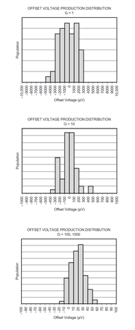
    This offset will be random on the onset of the usage of the device (i've provided the histograms for the offset voltage RTI across multiple gains). Generally for split supply circuits, both inputs can be grounded, then the difference between GND and output is measured to be the offset, and this is subtracted out in software by the microcontroller. It becomes slightly more challenging in single supply, as you will not be able to ground both inputs with a grounded reference voltage, since you will be outside the voltage range of the output amplifier.

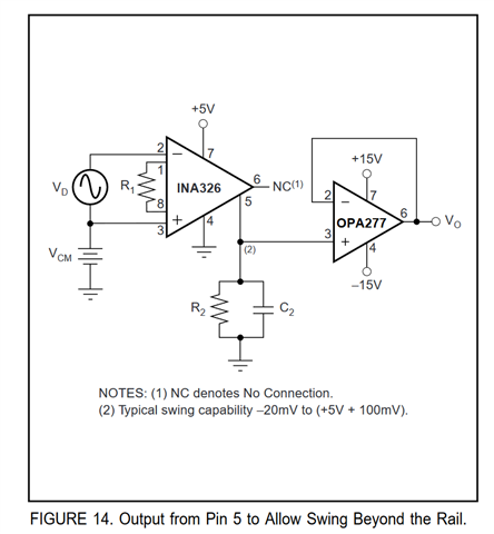
    If you are able to sense off of pin5, this pin can go up to 20mV below V-. In this case, for the majority of the offset voltage cases, you may zero both inputs, and you will see just the offset voltage on pin5. This allows you to not worry about the output swing from rail limit of the buffer amplifier. The example for this is shown on figure 14 of applications circuit.

    Best,
    Gerasimos

  • Thanks for the explanation, it makes sense. I just didn't notice the offset during the design phase. I'll be switching to a 1000Ω RTD and that should get the offset scale to manageable levels. I appreciate the time you took to make this clear.