This thread has been locked.

If you have a related question, please click the "Ask a related question" button in the top right corner. The newly created question will be automatically linked to this question.

OPA855: TIA Design with Bootstrapped Photodiode

Part Number: OPA855
Other Parts Discussed in Thread: OPA814, , TINA-TI

Tool/software:

Dear Support Team,

We are evaluating the OPA855 for use in a transimpedance amplifier (TIA) targeting 100 MHz bandwidth, with a total photodiode capacitance of approximately 100 pF (5×20 pF units) in a shunt bootstrapped configuration using the OPA814.

We have studied the relationship between photodiode capacitance and bandwidth, and have simulated the attached schematic in TINA-TI. So far, the simulation results look promising.

I have a couple of questions:

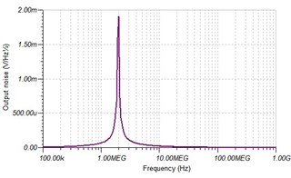
  1. Noise Peak at 2 MHz: In the simulation, a noise peak appears around 2 MHz. Increasing the value of C7 shifts this peak to lower frequencies but also makes it more pronounced. Is there a recommended method to mitigate this noise behavior?

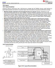
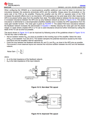
  2. PCB Layout Considerations: I’m planning to design a PCB for this schematic. Could you please review the design and let me know if there are any major concerns or common pitfalls I should watch out for—particularly regarding parasitic capacitance or any critical layout areas?

Any guidance would be greatly appreciated.

Best regards,

BootstrapTIA_OPA814_OPA855.TSC

  • Hi Mojtaba,

    I will look into it and get back to you.

    Regards,
    Aditya Gosavi

  • Hi Mojtaba,

    Regarding the layout for TIA, please check the section "10.5 Layout" in the OPA855 datasheet. This section provides detailed layout suggestions to minimize parasitic capacitance and inductance. 

    I am analysing the peaking seen at 2MHz, and will revert back as soon as I have any information.

    Regards,

    Aditya Gosavi

  • Hi Aditya,

    Thank you for your reply and for pointing out the layout section in the datasheet.

    Our goal is to integrate a bootstrap configuration in the TIA to reduce dependence on the photodiode's junction capacitance and achieve higher bandwidth. Therefore, I’m particularly concerned about layout considerations related to parasitic capacitances.

    I’m also not entirely sure if C7 is necessary, since the photodiode is AC-coupled to the TIA via C2. If the noise peaks above 100 MHz, we could potentially apply a simple low-pass filter at the output to remove it, given that our desired bandwidth is 100 MHz. What do you think?

    Regards,

  • Hi Mojtaba,

    We are looking into it and trying to understand your circuit, will get back to you as soon as we have any update.

    Regards,
    Aditya