This thread has been locked.

If you have a related question, please click the "Ask a related question" button in the top right corner. The newly created question will be automatically linked to this question.

THS3201: ths3201

Part Number: THS3201
Other Parts Discussed in Thread: THS3491

Tool/software:

Dear TI team,

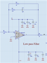
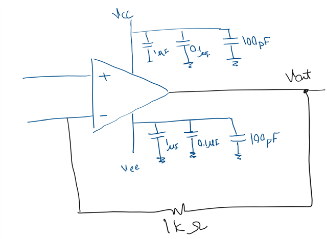
I am currently testing the THS3201 using the inverting amplifier configuration suggested in the datasheet,
...

but I am encountering unexpected behavior.

When powering the amplifier with ±7.5 V (Vs+ = +7.5 V, Vs− = −7.5 V):

The chip heats up significantly within seconds.
The output shows a clean ~300 MHz sine wave, even with zero input signal, and a dc offset is being added to the output signal despite having 0 offset at the input.

But! when switching to a single supply (Vs+ = 15 V, Vs− = 0 V):

The heating issue disappears.

However, the output still oscillates, now around 50 MHz, again regardless of input.


I tested this circuit in different conditions:

*.Tried multiple THS3201 chips to rule out damaged devices.

*. Tested with different feedback and gain resistor values, as suggested in Table 1 of the datasheet (e.g. Rf = 330 Ω, Rg = 110 Ω, etc.).

*.The power supply has been checked for proper voltage, noise, and current handling (by myself and other qualified personnel).

*.Input signal frequency was swept from kHz up to MHz ranges, and even when no signal is applied, the amplifier still produces high-frequency oscillations.

*.I used coaxial cables and proper SMA connections for high-frequency probing, and confirmed the setup using other known working systems.

*.The load at the output is a resistive load (~50 Ω or 100 Ω to ground), no load, or left open in some tests. Incase it was no load at the output and was directly connected to the oscilloscope I could see the input frequency with DC offset however (having 0 and 15V dc supply).

Additional Notes:
This circuit is part of a low-pass filter application, where the input signal may contain frequencies up to 10 GHz, though the output is expected to be under 300 MHz.
Layout is on PCB, and I am aware of the importance of transmission line effects at these frequencies, critical traces are routed as 50 Ω microstrip lines. However, I did the tests to up to 200KHz on breadboard, which should not be an issue.
Despite this, the oscillation appears to originate internally from the op-amp, not due to input signal coupling.

I would appreciate that if you could guide me on the probable reasons why these issues are happening and why I can't get the circuit working with the recommended dc supply values in the datasheet.


Looking forward to your response,
Best regards,
Mahsa

  • Hi Mahsa,

    This definitely sounds like a stability issue you are seeing. The device heating up and oscillating at the output despite any configuration changes are good signs of this. If you were able to test this device in a standard configuration with the recommended feedback resistors and still see the issues, then it is usually a layout concern. For the example you shared, Rf was 330ohms, which is relatively low for this device does increasing the value to say ~800 make a difference? Just for some clarity, were all these tests done on a breadboard or did you eventually transition to a PCB? 

    Best Regards,

    Ignacio 

  • Dear Ignacio,
    Thank you so much for your response.
    I did the tests on a breadboard, and used Rf up to 10 K. What I observed was that by reducing the Rf, say to 680, I could see the sine wave up to 500KHz and after that started to see distortion. But having Rf as 10K, the sine wave was seen up to 1 KHz or 70 KHz (depending on the Rg). That means that increasing the feedback resistor reduced my bandwidth.
    It is worthy to mention that all these result was recorded when having 0 and 15V for Vs- and Vs+, and could not see the results with -7.5 and +7.5. Shall I keep using 0,15V or it will cause issues?
    Moreover, I had offset in the output in all conditions, I would appreciate it if you could advice me on probable reasons for the offset and does it have something with oscillation?

    About the PCB that I mentioned, it was not a circuit from the datasheet. I tested the below circuit and still had the same issues (heating up with -7.5 and +7.5 and self oscillation).


    Best regards,
    Mahsa

  • Hi Mahsa,

    That does make sense, as with any current feedback devices, Rf will be the primary factor in the bandwidth of the device. Increasing Rf usually results in a more stable circuit, however bandwidth will decrease. The supplies should not affect the performance of the device. When switching from single to split supply the major consideration should be the input and output range of the device. If the input signals are centered around mid-supply in either configuration, the performance would not change. If you are seeing a major offset, beyond what would be expected by the internal offset of the device, it could be due to the oscillation. We have seen in the past the output of an amplifier settling to an erroneous DC voltage. For the circuit you shared, I would remove the 330ohm feedback branch as at higher frequencies, the net Rf value would be around 250ohms which is somewhat low for this device and could make this circuit unstable.

    Best Regards,

    Ignacio

  • Dear Ignacio,
    Thanks for your response and complete explanation.

    I completely removed the 330-ohm feedback branch, as you suggested, and tested the circuit again. Unfortunately, the issue persists. In fact, what makes this even more confusing is that I am using the exact circuit provided in the datasheet (Figure 55), and it still fails to work properly with ±7.5V supplies.

    Surprisingly, when I switch to a single-supply configuration (0V and +15V), everything works fine, and the amplifier operates as expected. This behavior is consistent across multiple tests, components, and even boards.

    Given that I’m running the exact reference design from the datasheet (which shouldn't oscillate), and I’ve carefully verified power supply stability and decoupling, and connections, I’m wondering why does the THS3201 only operate correctly with a 0V/+15V supply and not with ±7.5V, even when using the datasheet's suggested circuit?

    Additionally, I have not added any DC offset to my input signal in any of the tests, the input AC signal was always centred around 0V.

    Having these in mind, do you think I can continue using it with 0V/+15V safely, or is there something I’m overlooking?

    Thanks and best regards,
    Mahsa

  • Hi Mahsa,

    That is very helpful that you were able to recreate the figure in the datasheet. For the single supply configuration, having a signal centered around ground would violate your input common-mode range so I am not sure why this behavior would go away by setting the amplifier in single supply. For the configurations you set, did the amplifier show stability concerns when no input signal was applied and the amplifier simply biased?

    Best Regards,

    Ignacio

  • Dear Ignacio,
    Thanks for your reply.
    Today I tested the opamp in a simple biased circuit, as shown below:


    I'm seeing the output with oscilloscope,
    In dual supply mode (-7.5 and +7.5V):
    at the oscilloscope I'm seeing a signal at 135MHz, with 83mV peak to peak and 17mW power.


    in single supply mode (0,15V):
    at the oscilloscope, I see a noise-like signal, starting from 130mW power and going down to -3mW, having a peak to peak of 3mV.


    In both cases it heats up, I am using SOT-23 packaging, do you think changing the packaging to the bigger one would help?

    Thank you so much for your help,
    Mahsa

  • Hi Mahsa,

    The package should not be an issue and simply turning on the device without an input signal should not cause the device to heat up and oscillate. Could you share the PCB you are using. This is a very fast device and PCB layout is critical.

    Best Regards,

    Ignacio

  • Dear Ignacio,
    I tried this on breadboard. Do you think testing it on a PCB would solve the issue? and what are the consideration I shall take into account?
    Thanks,
    Mahsa

  • Hi Mahsa,

    Assuming the circuit was configured correctly like the circuit in the datasheet, I would say the issue is the breadboard. We see oscillations when breadboarding devices in the 200MHz range, a device in the GHz range will almost certainly oscillate. I would like to add that this device is not recommended for new designs, and we typically recommend the THS3491 as an alternative. As far as guidelines, there are some in the datasheet of the device starting on page 19. There is also a layout example later in the same section. For high-speed devices, one of the most important layout recommendations is to cut the planes under the inverting input pin and output pin. The layout in the datasheet highlights this. Short traces along with proper decoupling close to the board should also be implemented. We do sell an evaluation board for the THS3491 as well, which could be a good option for quick testing. I attached the EVM for that board below. It is a great resource for seeing how to layout your PCB.

    THS3491 EVM User's Guide

    Best Regards,

    Ignacio

  • Dear Ignacio,
    Thanks for your insight! I have used an SMD-to-DIP converter for the opamp, and the rest is on the breadboard.
    I would try testing the suggested circuit in the datasheet on PCB with your recommended layout soon and keep you posted. Hope it solves the issue.

    I completely understand your point, but what is important in my design is high bandwidth and low delay (low rise/fall time and high slew rate), which in both THS3201 has better performance, thats why I am keeping with THS3201, but if it could not operate, I would switch to THS3491.

    Moreover, I would like to have your idea on the inverting circuit of CFAs. 
    I came across an application report from TI,https://www.ti.com/jp/lit/an/sloa066/sloa066.pdf?ts=1749662721009, in which it is mentioned that
    '' The inverting configuration has extremely low input impedance, and therefore is not very useful. ''  
    I would like to know what 'not very useful' implies here? In my case, with a 50-ohm impedance, is the input impedance still low? And shall I switch to non-inverting configuration?

    Moreover, it has been mentioned that '' Current feedback amplifiers have a restriction—there cannot be any capacitance connected from the output to the inverting input.'', how if I use a capacitor seried with a resistor? Is it also not recommended?

    Thank you so much for your time and consideration.
    Best regards,
    Mahsa

  • Hi Mahsa,

    The PCB should help your circuit. Using any kind of adapter board will only add parasitics to the breadboard which is likely what you are seeing. The THS3491 EVM could be a good option if you would like to quickly test this chip. This device could be swapped onto the EVM. I am not sure what this comment on this app note is referring to. It is definitely not a high impedance input like a non-inverting configuration would be, but the device will still function in an inverting configuration. This second statement is referring to the minimum feedback resistance required for a current feedback device to function properly. As with any current feedback device, the bandwidth and stability performance will primarily depend on the value of Rf. If using a capacitor from the output to the inverting node, at high frequencies this path will be a short and the feedback impedance seen by this amplifier will be small and lead to stability issues. Having a capacitor as a feedback branch with a series resistor should work as long as the total feedback impedance value is in the ideal range of that current feedback device.

    Best Regards,

    Ignacio