This thread has been locked.

If you have a related question, please click the "Ask a related question" button in the top right corner. The newly created question will be automatically linked to this question.

TSV914: TSV914 OP-AMP

Part Number: TSV914
Other Parts Discussed in Thread: TLV9054

Tool/software:

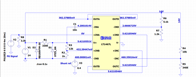
We are currently using the TSV914 operational amplifier in place of the LT1467L in a fault-detection application. Our objective disable the signal output in the event of overvoltage, overcurrent, or high temperature conditions.
During testing, we encountered the following issue:
  • The output of the op-amp was showing an unexpected offset voltage of ~3.4V.
  • To resolve this, we added a 100Ω resistor in series between Pin 14 (OUTD) and Pin 1 (OUTA), which helped bring the output offset down to 0V.
However, we are still facing a critical issue:
  • During a fault condition, Pin 13 rises to 5.8V (above the reference of 5.6V), yet the output remains high, whereas we expect the output to go low to disable the pulse signal.
We would appreciate it if you could help us understand the cause of this behavior and advise on:
  1. Whether this configuration is valid for fault signal suppression,
  2. Why the output does not respond correctly to the reference threshold being exceeded,
  3. Any changes or recommendations for reliably achieving output cutoff during fault conditions.
We are attaching our schematic for your reference
  • Ilavarasan,

    There are a few unusual things in this schematic. 

    -INA has no DC bias. On LT1467L there is high bidirectional bias current so it will settle on a 'within power rails' voltage in a short time. TSV914 has "no" bias current, so voltage will drift to a random voltage after a potentially very long time.  

    Two outputs shorted together so they can fight for an unknown output voltage and draw V+ supply voltage down. (unreliable operation and chip might get hot)  

    All channels used as comparator, but chip is an op amp. (sometimes not harmful)

  • Ron Michallick,

    Thank you for your information, is there any other alternative way to achieve this kind of output?

  • Ilavarasan,

    What is the desired purpose of CH1 and C1?

  • Ron Michallick,

    C1 is used as a Bias for -INA using the V+ ( now I understood this doesn't provide DC bias to -INA)

    I am working on a circuit designed to drive an IGBT gate driver using a pulse input. The goal is to disable the pulse signal when any one of the following fault conditions occurs: overvoltage (CH4), overcurrent (CH2), or high temperature (CH3).

    In my design:

    The pulse input is connected to CH1 and used to drive the IGBT gate driver.

    CH2, CH3, and CH4 are connected to separate op-amps configured in series for fault detection.

    If any fault condition is detected, the output pulse to the gate driver should be cut off.

    The circuit worked well during simulation. However, during testing, I faced an issue with the output, as previously mentioned. I would appreciate your advice on how to achieve the expected behavior in the actual hardware.

  • I am working on a circuit

    Present tense leads me to think that this isn't working (properly) even with LT1467. 

    Regardless of that, is a schematic and resulting circuit board change a acceptable path forward?

    What levels are considered "overvoltage" at source, "over current" at sense resistor, input from "over temperature" ?

  • Ron Michallick,

    Thank you for your support so far.

    LT1467 is used in LTSpice for simulation only we don't have this part in our hand to test. We are using only TSV914 for testing.

    Nomial operating voltage 14V overvoltage detection at 30V Over current at 8A and over temperature at 150C

    I have tried a wired diode AND configuration as below now i can achieve the expected output, can i continue to use this configuration with TSV914 or there is any other better option to do this.

  • Ilavarasan,

    For a supply that could reach 30V and for a more accurate refence voltage, I suggest using TPS7B91050DBVR to get 5V and replace D2, D1.

    -INA still needs a DC voltage. 

    overvoltage detection at 30V Over current at 8A and over temperature at 150C

    Will any or all of these need hysteresis? Hysteresis can prevent erratic (glitchy) pulse output when near the thresholds (of OV, OC, OT)? 

  • I suggest using TPS7B91050DBVR to get 5V

    Noted, Already replaced with a 5V LDO

    -INA still needs a DC voltage. 

    Noted, Will add a voltage divider from v+

    Will any or all of these need hysteresis?

    One hysteresis can be used at OUTD to reduce the glitches during fault detection (Low signal). 

  • I think each stage needs it own hysteresis. Here is my version, lightly simulation tested.

    I used TLV9054. All four comparator have the ability to make output low.  All must want high for output to be high. 

    TLV9052 Chain.TSC

  • OK, to change R11 to a diode then make R12 bigger, like 20k.

  • Thank you for your suggestion, will try out this configuration.