This thread has been locked.

If you have a related question, please click the "Ask a related question" button in the top right corner. The newly created question will be automatically linked to this question.

AMC3302: Current measurement inconsistenties in redundant system

Part Number: AMC3302
Other Parts Discussed in Thread: AMC3330

Tool/software:

Dear TI experts,

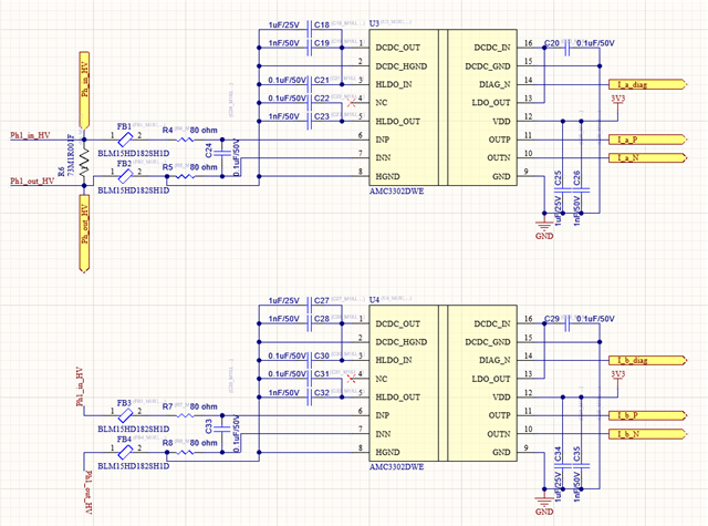
 We created a circuit to measure the three phase currents in a servo motor system using the AMC3302 ICs. For each phase, we created a dedicated measurement in a redundant structure as you can see in the schematic below. Given this system we deviated slightly from the standard operating procedure for other reasons:

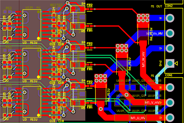
  • We connected 2 AMC3302 ICs to the same shunt resistor for a redundant measurement system
  • We placed the AMC3302 ICs that are measuring from the same shunt in a stacked orientation (https://www.ti.com/lit/an/sbaa515a/sbaa515a.pdf?ts=1754307985947&ref_url=https%253A%252F%252Fe2e.ti.com%252F)
  • For different measurement reasons and observations, we reduced the number of ferrite beads from 3 to 2 per AMC3302, and connected HGND to INN in front of the differential input filter (80ohm and 100nF)
  • We used a six-layer PCB and extended the ground plane in all layers all the way to ferrite beads and underneath the AMC3302 ICs to shield interference from the stacked AMC3302 at the bottom layer, as well as to shield interference from voltage signals running between the stack (thin green lines in layout)

Given this setup we are experiencing 2 problems. At first, we are experiencing inconsistencies over different phase current measurements during calibration of all phases. Four out of the six measurements are consistent with each other, whereas two completely differ. However, the layout for all of them contains differences. Nevertheless, we did not expect to any current running from the shunt over the PCB trace to the ferrite beads and differential input filter. Therefore, we are curious in which way this problem could be related to the layout. Would you be able to give us some suggestions for debugging?

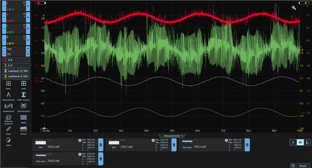
Secondly, when measuring with our oscilloscope, we also observe a lot of noise being accumulated across the differential input filter capacitor. In addition, in a high-noisy environment the impact of the noise continues to grow. Is there any reason that you can think of that could impact the noise in your opinion on all of these AMC3302s? For your reference, we are also using the AMC3330 for voltage measurements on the same board, and the impact of noise on this IC is much smaller. Is this related to a difference in input resistance between both ICs?

 We are hoping for a fast response and would appreciate any feedback.

Gertjan

Schematic of measurement setup:

Layout of measurement setup:

  • Hi Gertjan,

    What do the inconsistencies and noise you are seeing in your system look like? Did you take scope shots that you could share of these behaviors? 

    Can you please elaborate on the ground planes you mention running under the AMC units? It appears your ground plane extends from the high-side to low-side of the device. Where are the devices connected to the ground plane? Do you have a layout picture of the bottom traces as well? And layouts that include the shunt connections?

    Having a connection across the isolation barrier can compromise the isolation barrier and lead to unexpected behavior. Compromising the isolation barrier can also pose an electrical risk to the device. 

    Best regards,

    Eva

  • Hi Eva,

    Thanks for your follow up, let me try to answer to you as good as possible. We started with a simplified HW module, using the same schematic, as a first iteration of a prototype board, and then moved forward to the board discussed in the previous post. The only difference between both versions resides in the HW layout. We tested the measurement of the prototype and the new board side-by-side and you can find the side by side measurements in the plot below (old HW red, new HW green). We saw a clear increase in noise originating from the board with the new HW layout.

    I think on the previously shared picture, you can already see the shunts (R6_xxx), and the bottom traces in blue. The devices connected to the ground plane are power converters, opamps, and multiplexers.

    There is indeed a ground polygon in all layers of the PCB which is connected to pin 9 and 15 of AMC3302. However, all components on the HV side are not directly connected to the ground polygons. Nevertheless, as you can see in the above layout, the ground polygons are stretched out along the AMC 3302 and the HV components and could be coupled capacitively to them. Therefore, we would like you (1) to comment on the impact of noise versus the clearance area, to be kept free of any conductive materials underneath the AMC3302, (2) how to handle it if two AMC3302s are stacked on both side of the PCBA, and (3) how to shield other signal traces that are running below the AMC3302.

    Kind regards,
    Gertjan

  • Hi Gertjan,

    Are the ground planes the only layout changes between the two iterations? Having the ground planes running under the entire AMC devices is likely the main reason for the difference in the two results. 

    I think following the layout best practices in the app note you previously linked is a good resource Best Practices to Attenuate AMC3301 Family Radiated Emissions EMI (Rev. A)

    Best regards,

    Eva

  • Hi Eva, 

    Thank you for the suggestion. Can you describe the effects that a ground plane underneath the AMC3302 could have such that we can cross check this hypothesis and start with the redesign of the board? What could be the source of this generated noise and which frequency signals would you expect to be dominant given the design of the AMC3302?

    In addition, we are wondering what is meant in the best practice guide in the section regarding the stack-up. Is pin 4 (AMC3302's datasheet mentions it is NC) used in this example, and are both stacked AMC3302s connected together at pin 2 and pin 8? Could you help us interpret this description in the guide? If pin 2/8 of stacked ICs are connected, does that mean that the pin 2/8 of nearby AMC3302 and AMC3330 should also be connected to the same node?

    Kind regards,

    Gertjan

  • Hi Gertjan,

    Would you have a schematic/layout including your current design with the AMC3330? If the two devices are measuring the same shunt, the HGNDs can be connected but otherwise shouldn't be. 

    Another source of noise to look into could be the sensing connections. Did you add a plane over the shunt sensing connection pads? Asymmetrical sensing connections and not following a shunt resistor's recommended connections can lead to noise as well. 

    Best regards,

    Eva