AMC3302: DC bias offset at zero load

Part Number: AMC3302

Tool/software:

Hello, I have observed a DC bias offset at AMC3302 IC input in our design used for current sensing.

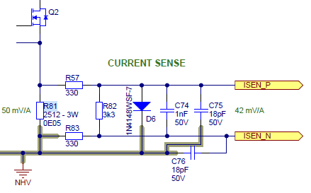
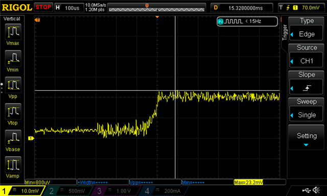
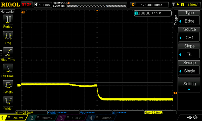
The +17mVDC offset is quite large with respect to the maximum full scale linear differential input voltage of ±50mV and way more than the datasheet specified ±50µV.

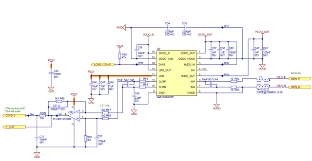
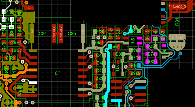
The design incorporates multiple galvanic isolators for 4 isolated nets by means of transformers, optocouplers and the iso-opamp AMC3302, effectively isolating SELV and LIVE parts.
The offset becomes present when +24VDC is supplied on the SELV side, without connecting any loads or enabling any isolated nets.

Basically, only +3.3VDC is supplied to VDD.

Do you have any advice or idea please?


Thank you in advance and best regards,


Fabien

  • Hi Fabien,

    Have you tried disconnecting the device inputs (remove r62 and r65), shorting the inputs at the device, and checking if the offset is still there?

    Thanks.

  • Hi Saleh,

    Thanks for the feedback.

    Tested three different setups.

    # Measurement @L5 @pin6-7 INP - INN @p11-10 OUTP - OUTN
    1 R62 and R65 removed 0 V 0 V 0 V
    2 Only R65 removed (R62 placed) 33 mV -239 mV -2,5 V
    3 Only R62 removed (R65 placed) 0 V +249 mV +2,5 V

    #2 and #3 respectively @pin6-7 INP - INN.
      

  • Hi Saleh,

    Shorting both R57 and R83 solves the +17mV DC offset at input INP - INN.

    Shorting either one resistors halves the DC offset.

    It is unclear to me at this point whereas the DC offset originates no HV section power supplies or loads are active.

    To protect the isolation amplifier against a shorted load some additional components are added. Resistor R57 limits the current flowing to the amplifier. R87 is used to keep the circuit symmetrical.
    Shorting the resistors disables opamp protection against shorted load and is therefore undesirable.

    Awaiting your response.

  • Hi Fabien,

    The offset is likely due to the input bias current of the device, which is around 36uA typical.  That bias current goes between the input pins and HGND, so an offset voltage will be generated as the bias current goes through any resistance in the path.  I think if you replace R57 and R83 with 0Ohms, the offset should go away (INP to HGND: R62+R57+R81+R83+R65 = 680Ohm; 36uA * 670Ohm = 24mV DC offset).

    Also, typically you want to make the HGND to INN connection at the current sense element for better noise immunity.

    Thanks.