Tool/software:
Hi Team,
We are using the OPA196IDBVR in our design and need clarification regarding its input offset voltage drift.
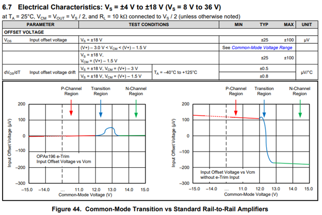
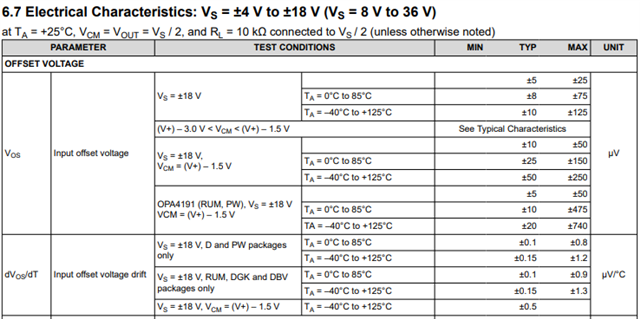
According to the datasheet, the typical value is specified as <0.5 μV / ⁰C at VS=±18V, VCM=(V+)-3V, but there is no maximum value provided.
Could you please confirm:
- What is the maximum input offset voltage drift at VS = +12 V / -10 V, VCM < (V+) - 3 V?
- If this information is not available to share, otherwise could you recommend a pin-to-pin compatible operational amplifier with a guaranteed maximum input offset voltage drift of <0.5 μV/°C that can be used as an alternative to the OPA196IDBVR?
Your support will be greatly appreciated.