INA180: Power leaks from input pins to VCC pin

Part Number: INA180


Hello TI Team,

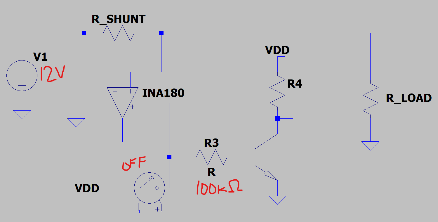
Because this part allows the common mode voltage to be so much greater than the VCC voltage, I assume there is separation of these two nodes in the internal circuitry.

However, I am noticing that voltage appears on the VCC pin whenever there is voltage on the input pins (and the IC is unpowered).

Below is a simplified version of my circuit: the INA180 is powered down to reduce system Iq (battery powered), but the BJT circuit will turn on due to this parasitic voltage on the VCC pin.

Is this expected behavior? I guess I could resolve it with a pull-down resistor on the VCC line, but I don't like wasting energy if not necessary.

image.png

Thank you!

-RB

  • Hello,

    Sorry for the delay.

    Internally the INA180 will allow some amount of current to flow through the input pins during shutdown according to the datasheet:

    This will flow to GND and the output according to the schematic shown in the block diagram:


    However I would not be surprised if the ESD diodes or other internal circuitry provide a path for the input bias current to flow to VCC as well.

    The current level should have a maximum of about 0.1mA from both pins, so this is probably the worst case current you could expect to the Vs pin (though it is probably lower).

    Have you made any measurements to determine the voltage you are seeing on the output? This would help determine the pull down resistor strength to optimize for your power requirements.

    Let me know if you have any more questions,

    Levi DV