This thread has been locked.

If you have a related question, please click the "Ask a related question" button in the top right corner. The newly created question will be automatically linked to this question.

TLC2272A: Difference in Offset value depending on the marking done (packaging site =different specs?)

Part Number: TLC2272A
Other Parts Discussed in Thread: AMP-PDK-EVM,

We have used since +10 years P/N TLC2272AID(R) in industrial products with no issues. Recently we received a batch (sourced directly from TI) with different marking: Instead of a Texas logo drawing (as usual and no issues) they came with the letters TI before the P/N. Those parts have more offset than the usual ones causing troubles in the circuit behavior. We have done several replacements of parts and all the TI marked have this offset out of specs: Instead of 1-2mV they have up to 12mV.

I have seen these P/N could be packed in TAIWAN and AGUASCALIENTES. 

Can somebody help us to understand what is happening and how to face this issue?

Thanks, Jose Luis 


  • There was a PCN, but 12 mV is beyond anything reasonable, even for worse opamps. What is the marking?

    Is this the input offset? How exactly are you measuring it?

  • We are an EMS, we source parts, assy, and test PCBA´s.

    According with our customer (designer & final user) they use this P/N as a buffer (1 gain amplifier). with 0V at the input they measure up to 12mv at the output.

    One marking examle is (in three lines):

    2272AI

    TI52M

    A34V

  • Hi Jose,

    I'd be happy to help with this. 12mV of input offset voltage is considerably higher than I would expect for this device, so I would like to verify that the test circuit the customer is using to measure the Vos matches the conditions defined in the datasheet. 

    For reference, the part marking change PCN was sent out in 2022 (PCN 20211123004), and CFAB was added as an additional FAB site in 2023 as part of TI's transition to newer and more efficient manufacturing sites (PCN 20230130003.1). These two changes are separate, so not all devices with the new marking were produced after the fab transition. 

    Please clarify the following:

    1. What are the supply voltages of the amplifier? 
    2. How exactly is the customer performing the VOS measurements? Are they using a dedicated test circuit or measuring in their application circuit? A schematic of their measurement setup would be very helpful here.
    3. How many units has the customer measured higher than expected VOS on? Does the issue seem to be isolated to a specific lot of TLC2272AIDR? 

    Best Regards,

    Alex Curtis

  • Hello,

    I´m the customer.

    The problem we are experiencing is having 0V at the input of the OpAmp, we are measuring about 12mV on the outpput. The OpAmp is set as a buffer, with gain 1, and is supplied with a single 3V3 power.

    Seems only affects to batch:

    TI52M

    A34V

     thanks

    Iván

  • Hi Iván,

    Thank you for clarifying your observations. 

    How many units within the batch have shown output voltages of 12mV? And are you using a separate, dedicated circuit to measure the offset voltage? I want to rule out if the circuit you're using to measure the output could be contributing to the higher than expected offset voltage.

    Best,

    Alex Curtis

  • Hi Iván,

    After further consideration, the output of the opamp is approaching the low level output voltage of the device in the configuration you've described. 

    Could you measure the offset voltage with a split supply configuration (such as +/-5V) instead of single supply?  

    Best Regards,

    Alex Curtis

  • Hi Alex,

    Sorry,we are not able to measure with a split supply.  

    About the quantity, we have tested about 10-12 units of that batch, and all of them have the same behaviour.

    Maybe the Max. Negative Peak Out could be the reason. In our application, Io=1.5mA

    Thanks!

  • Hi Iván,

    To accurately compare against a specification in the datasheet, the operating conditions also need to match, so without placing the amplifier in a split supply I'm unable to determine if there is a problem with the offset voltage or if the amplifier is operating within specification. 

    When you measured the output voltage of 12mV in the circuit you've described, what is the load impedance connected to the output? I agree with you that driving higher output current would further limit the low level output voltage and could explain the behavior you've observed.

    Best Regards,

    Alex Curtis

  • Hi Alex,

    ok, we will try to measure against datasheet specs. As soon we have results, I post them.

    The load Impedance is about 1.5mA.

    Regards!

  • Hi Iván,

    I'm looking forward to your next update. In the meantime, if there's anything else I can assist you with, please let me know Slight smile

    Best,

    Alex Curtis

  • Hi Alex,

    as soon as my mates perfom the tests, I post the results.

    Thanks!

    Regards

  • Hi Alex,

    sorry for late reply.

    Last week, my colleagues could perform some measures (keeping the follower topology) and these are the results:

    Split Supply - Vo:

    5+- 385,2mV
    4,5+- 355.3mV
    4+- 325.1mV
    3,5+- 295,2mV
    3,3+- 283,1mV
    3+- 264,8mV

    Single Supply - Vo

    5 1,1mV
    4,5 0,4mV
    4 1,1mV
    3,5 5,4mV
    3,3 9,2mV
    3 19,1mV

    Those measurements are what you expected??

    Regards

    Iván

  • Hi Iván,

    Thank you for sharing these measurements, although a higher offset voltage in a split supply configuration is not what I would expect, so I would like more information on your measurement setup.

    1. To clarify, did you use a separate board to test the offset voltage (like the DIYAMP-EVM or AMP-PDK-EVM) with the amplifier in a buffer configuration, or were these measurements taken with the amplifier in your application circuit?
    2. Could you confirm what the output of the amplifier is connected to? 
    3. Were both sets of measurements taken with the amplifier driving a load current of 1.5mA? 

    Best Regards,

    Alex Curtis

  • Hi Alex,

    We extracted the OpAmp and mounted/welded in a separate proto-board, trying to simulate the original circuit.

    The output is conected simply to a resistor (2K Ohm) . The original circuit is a resistor in parallel witth the input of an ADC.

    A think I express wrong the load current. Usually the working load will be near of 1,5mA, but with the input at 0V, the output should be 0v, so the current is minimum. We have repeat the test and these are the results:

    Single Supply Output
    [mV]
     (Io)
    [uA]
    5 1,0m 0.6u
    4,5 1,5m 0.8u
    4 2,7m 1,2u
    3,5 6,1m 2,6u
    3,3 9,2m 3,7u
    3 17,6m 6,9u
    Split Supply Output
    [mV]
     (Io)
    [mA]
    5+- 383,1 1,72
    4,5+- 353,4 1,54
    4+- 323,6 1,37
    3,5+- 293,7 1,19
    3,3+- 281,7 1,12
    3+- 259,9 1,02

  • Hi Iván,

    I have units of the TLC2272AIDR and I measured the input offset voltage at approximately 408uV.

    I put the amplifier in a split supply configuration (+/-5V), in a non-inverting gain of 101V/V, using the AMP-PDK-EVM and the SOIC-8 daughtercard, connected as shown in the AMP-PDK-EVM user guide: 

    I measured -41.25mV on the output of amplifier 1 which corresponds to an input offset voltage of -41.25mV/101 = -408uV, which is very close to the typical spec of 300uV. Adding a 2kOhm load resistor did not change the measured output voltage. 

    I then placed it in a buffer with the non-inverting input connected to ground, and a 2kOhm resistor connected to the output. With a split supply of +/-5V, I measured -403uV across the 2kOhm resistor. In a single supply configuration (+5V), I measured +358uV across the load resistor. 

    Could you measure the output voltage in the dual supply configuration again, but with the load current close to 0A like you did for the single supply? This would indicate if the input offset voltage is within the expected range for the units you have.

    Best Regards,

    Alex Curtis

  • Hi Alex,

    here goes the values:

    Output
    [mV]
     (Io)
    [uA]
    0,9 0,1
    0,9 0,1
    0,9 0,1
    1 0,1
    1 0,1
    1 0,2

    The Vsupply goes from +-5 to +-3v3 as other measures. 

    Thanks in advance.

  • Hi Iván,

    Thank you for taking these measurements, and my apologies for the delayed response.

    Given that the maximum input offset voltage for this device is 1.5mV (1500uV) in a +/-5V split supply configuration, these results indicate the device is operating within datasheet specification

    To bring this back to your original issue, I understand the output current in your application is typically 1.5mA, and as we've discussed, the input offset voltage will increase as the output current of the amplifier increases. If you require a lower offset voltage, I would suggest either limiting the current the opamp needs to drive, or using an amplifier with a lower maximum offset voltage specification that meets your performance requirements.

    If you would like to consider alternative amplifiers, I would be happy to provide recommendations. Let me know how you would like to proceed Slight smile

    Best Regards,

    Alex Curtis

  • Hi Alex,

    Thanks for your reply. 

    OK, totally understanded.

    The problem is not critical, so the otuput is acceptable. In any case, I would like to take advantage of your proposal, so, could you provide some alternatives in order to test it and thus be able to decide ??

    Thanks in advance!

    BR,

    Iván

  • Hi Iván,

    I am a product marketing engineer working with Alex Curtis on this inquiry. I would like to help you find a suitable alternative to TLC2272A that has improved input offset voltage (especially when driving higher load currents).

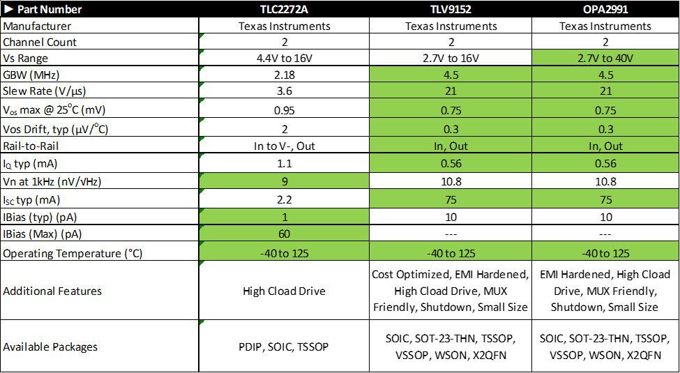
    To start, let’s consider TLV9152 and OPA2991. This is drop in next generation to TLC2272A.

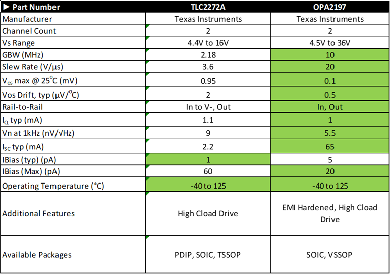
    For a substantial improvement in offset voltage, you could consider our newest zero-drift amplifier (TLV2886) or an industry standard e-TrimTm device (OPA2197)

    Let me know what you think and if there are any further questions we can address.

    Best,

    Jack Snyder

  • Hi Jack!

    Thanks for your help. I will check all the info about the proposed references and we will test the selected ones. 

    Best regards

    Iván