This thread has been locked.

If you have a related question, please click the "Ask a related question" button in the top right corner. The newly created question will be automatically linked to this question.

Transimpedance amp output is unstable

Other Parts Discussed in Thread: OPA381, OPA830, TS5A3160, OPA333

Hi,

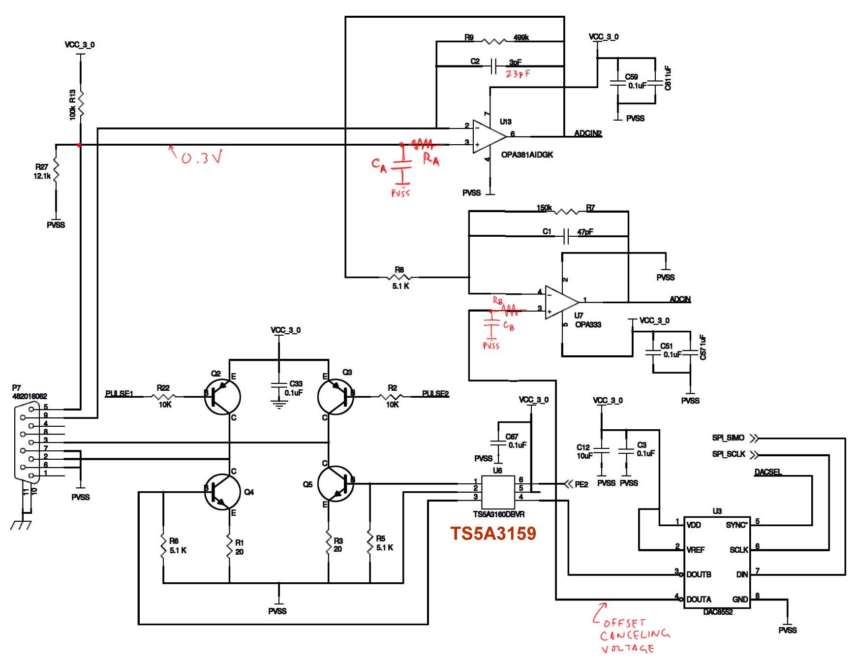
I'm using an OPA381 as the first stage of a pulse oximeter amplifier similar to the circuit in this app note SPRAB37 and shown below. Its output goes unstable as I increase LED brightness (which increases photodiode signal). I am showing this design first as it is ostensibly a known working design (our design is shown next):

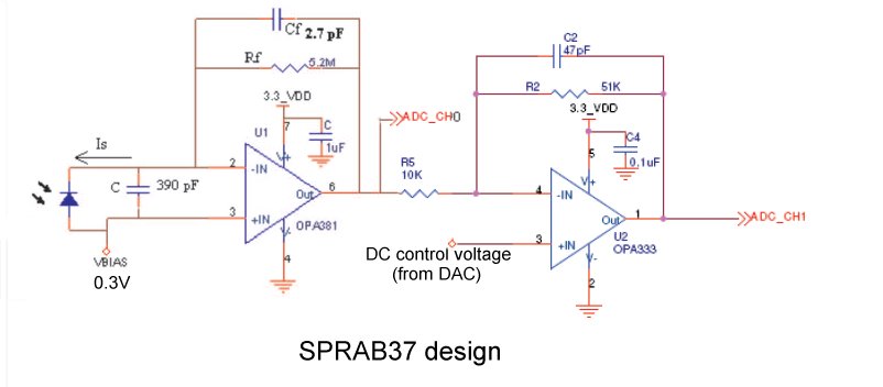
This design was subsequently ported by TI to MSP430 with internal op amps and has two different revisions, finalized in this version:  SLAA274B.

We moved from MSP430 design back to external op amps. Notably, key components were changed in the MSP430 design. We kept some of the changes made in the MSP430 design and arrived at our design below. Note the most differences from the original SPRAB37 design are highlighted in red:

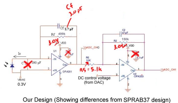
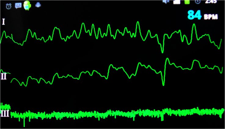
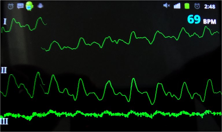
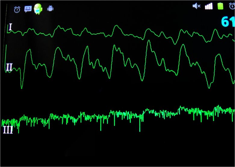
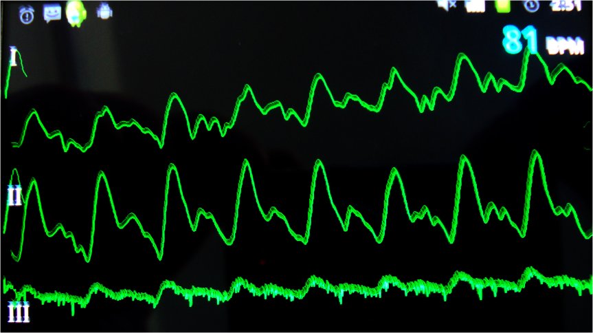
We have been incrementally changing the gain in both stages (R2 and Rf) to try to get a stable signal that can read pulse oximeters for various skin types. Our basic problem is our 1st stage goes unstable as we increase LED brightness before we can get a good signal for darker skin.

Here is our background:

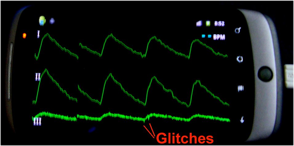
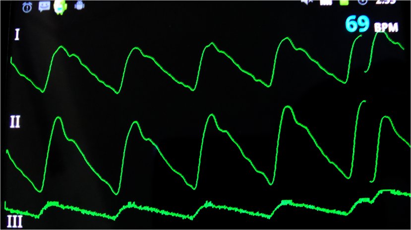
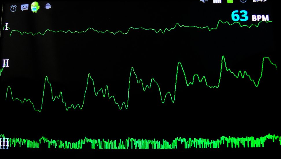
  • We can now get a good pulse ox signal for light skin with good circulation.
  • To do this we have iterated Rf and R2 feedback resistors and manually change  the offset (DC control voltage) in the second stage and the LED intensity into the first stage photodiode. 
  • We also tried adding back the 390pF cap in the first stage input (no improvement). 
  • We dropped our gain in the second stage down (because we were clipping on 0 and 3.0V rails) from R2 = 150k to R2 = 38k. 
  • We had upped the gain in the first stage to Rf = 5.1M before we realized we had the wrong op amp (we found we had the OPA830 instead of OPA381 in the first stage...this has been fixed.) 
  • Now we have moved it back down to Rf = 1.7M. Although this works great for my very pink translucent fingers, it does not work well for the browner members of the team. 
  • The output of the first stage begins to oscillate as I increase the diode brightness before I can get a good signal. I am moving from 1.7M to 1.3M at this point. 

What I really need is a transimpedance op amp expert to comment on this to tell me how to calculate or choose my Rf Cf and R2 and whether we need any cap on the input. I know that transimpedance amps are tricky, but I thought working with two previous designs would narrow my design down a bit. It has, but I have yet to arrive at an optimum solution. Currently R2 = 38k and Rf = 1.3M.

One other thing: Thanks in advance for your help!!!!!

Kind regards,

Kevin Kreger

  • Kevin,

    Please allow us some time to study your application. We will get back to you as soon as we have some comments.

  • Kevin,

    The feedback resistor in your transimpedance amp should be selected according to maximum current signal from your photodiode. If your maximum light level signal is not yet causing the input amp to swing near the 3V supply voltage, you can increase the feedback resistor. It its output voltage is "hitting the top rail" at maximum light level, you've gone too far.

    An external capacitor across the photodiode is undesirable. Nothing good can come from this. We try to minimize capacitance across the photodiode. The feedback capacitor, Cf, is probably okay. Assuming the OPA381 is not oscillating, there is probably no reason to change this value.

    I'm concerned that the 1uF power supply bypass capacitors have been eliminated. Why? This could be a cause for oscillations.

    In general, it's best to put as much gain as practical in the first stage, the transimpedance amp. Get that amplifier working properly by looking at the output on a scope. Verify no oscillations and good signal swing on this stage. Then add additional gain in the second stage as needed to get desired output to the a/d converter.

    Regards, Bruce.

  • Hi Bruce,

    Thank you so much for your advice! As I mentioned the design was migrated from the MSP430 design having internal op amps. The original design having the caps was consulted afterwards, hence the miss on the 1uF bypass caps. It was not intentional and they will be added back post haste per your advice! :-)

    We found out the cap across the photodiode was a bad idea by trying it out as well.

    Once we add the 1uF bypass caps we will see if the oscillations are eliminated and then tweak the gain again as you suggest by observing the level at which we reach full scale with maximum LED intensity.

    Finally, we will add gain back to the second stage.

    Bruce....it seems like you've nailed it. I will let you know what happens based on the design mods and experiments you have advised.

    All the best.

    Kind regards,

    Kevin

  • Hi Bruce,

    First of all, adding the 1uF bypass cap definitely helps. Now I have had to rollback the 5.1M Rf on the first stage until I get back to 500k (actually 499k) for stability from oscillation and to reduce noise glitches. This eliminates all of the instability/noise in the first stage when I am only pulsing a single LED (infrared or red) at 500Hz. However, if I multiplex/interleave the red/infrared pulses (1kHz total) I get some glitch noise back (but it does not cause the oscillations as before). Another engineer suggested that I try to increase Cf to 9pF or so. Do you think this is a good test? I could see the glitch noise decreasing as I decreased Rf and I can still get it back if I increase the LED brightness as well.

    Thanks again!

    Kind regards,

    Kevin

  • Kevin,

    It seems that increasing the Cf to 9pF would still give you plenty of signal bandwidth relative to your 500Hz modulation frequency so this may be a good change. A scope picture of the "glitch" would greatly help in judging the problem. Glitches can take many forms and details of the appearance can reveal much about the possible cause.

    Regards, Bruce.

  • Hi Bruce,

    Increasing Cf did not help, but I'm pretty sure I understand why after reading this app note from TI:

    http://www.ti.com/lit/an/sboa055a/sboa055a.pdf

    When I increased Cf from 3pF to 6pF the output went to the rail as it was integrating more current.

    BTW, my values for Cf = 3pF and Rf = 499k are nearly the same as in the most recent TI app note's pulseox circuit (3pF and 500k resp.).

    It may just be the difference in capacitance of the photodiode had made my circuit sub-optimal. Here is a shot of my pulse ox signal:

    The glitches I am seeing are small when I look at my finger's signal. The top two signals above are the filtered output of the second stage of the pulse ox circuit...the Red and Infrared diodes are top and middle. The bottom is the unfiltered infrared wherein I've indicated some small glitches. There rest all is 50/100Hz noise from ambient light and EMF...this is mostly filtered out, but I get these intermittent noise glitches. This capture is not a real good example because it is not a bad case (everyone is out of the office but me and I have a great signal). With others who have a smaller signal the glitches are sometimes the height of the peak of the pulse ox, but other wise look the same...spikes that are about the width and totally random...sometimes more sometimes less.

    In general, I think I can solve the problem by applying a stronger digital LPF, but I'm getting less signal with darker skin or poorer circulation, so I have to do some more testing to see if I can increase the diode brightness sufficiently enough to override the noise without sending the op amp into oscillation. I feel that I am close, but I am still trying to get mfg data on the photodiode capacitance and resistance so that I can tune the values per the app note referenced above if I am not able to get a good signal from darker skin.

    Thanks!

    Kevin

  • Kevin,

    The glitches appear to be very narrow with little energy present. Their frequency content is very high compared to your fundamental signal frequency so it should be easily filtered. I still believe that you could benefit from a higher value of Cf.

    The application note you are citing primarily deals with stability issues. I don't think this relates to your problem. The purpose of increasing Cf is to act as a filter. This will help to control the glitches. I suggesting trying Cf=20pF.

    A possible source of the glitch is the 0.3V bias voltage or the offsetting DAC voltage. Noise on these voltages will feed through as signal. You have not described how these sources are created. You may want to try filtering these voltages.

    Regards, Bruce.

  • Hi Bruce,

    Thanks for the prompt response (and on the weekend again!). I admit I was put off when I added 3pF and it railed, but I will try again with 20pF per your suggestion. Yes the glitches are narrow especially w.r.t. my low frequency of interest. They can get quite large, as I mentioned the height of the pulseox signal.

    However, you have also given an excellent suggestion about filtering my 0.3V reference. This output is a 100k/12.1k voltage divider from a 3.0V regulator (that also drives an ECG circuit). I am already adding a significant filter to this in the next revision because I was getting pulse ox switch noise on my ECG circuit (and have been given advice by another TI engineer on e2e). As far as noise from the offsetting DAC voltage, this could be a potential problem as well. Given I switch two voltages onto this input at 500Hz do you have any suggestion for a cap value to try on this input?

    I think the 0.3V or DAC may be the source of much of the noise (now that you have pointed it out :-)

    Finally, I will increase the rejection of my LPF. I just want to make sure the hardware is optimized first.

    Kind regards,

    Kevin

  • Kevin,

    The DAC is driving a high impedance node so you can easily add series impedance. Also, if your DAC can provide more voltage than you need, divide this voltage down with a voltage divider to minimize the noise from this source. Make the impedance of the divider around 10k or so. Then add a 1nF capacitor to ground.

    Regarding the added feedback capacitance on the TIA, I can't think of a good reason why that additional 3pF caused the output to rail. I suggest that you for forget that experience. I believe that it was probably a flawed experiment.

    Regards, Bruce.

  • Hi Bruce,

    Thanks for the follow-up! The DAC is a dual channel that drives both the bases of the transistors in the LED drive circuit and it sets the DC offset. These two channels are switched at a 1khz rate. I can divide the DAC that drives the transistors by half. I cannot divide the DAC that drives the DC offset as I am uncertain what the maximum offset cancellation that will be needed but, on paper, it could be as much as 3.0V (the max out of the DAC). And I can add series impedance to both DAC outputs as you suggest.

    I will 'forget' the encounter with the flawed experiment and increase the capacitance.

    Thank you for pointing out what should have been obvious!

    Kind regards,

    Kevin

  • Hi Bruce,

    Well, it was a failed experiment. I added 10pF and got a better response and then another 10pf (for a total of 23pF) but it looked like a case of diminishing returns. Some of our spike noise was eliminated by adding a 1.0uF bypass cap along with the 0.1uF.  

    Finally, when I use a darker skin patient I have to turn up the LED and it un-stabilizes the output of the first stage before I can get a usable signal. At first I see lots more of the 50/100Hz 'hair' because the signal is lower, but as I increase the LED brightness, the signal ~starts~ to get a better SNR, but then it goes unstable without oscillating or clipping. I'm not sure if I should reduce Rf in the first stage.

    Thoughts?

    Thanks again Bruce!

    Kevin

  • Kevin,

    It sounds as if you are struggling with the problem of a relatively small AC signal riding on a large and variable background DC signal. Please read this thread and see if any of this rings true to your situation.

    http://e2e.ti.com/support/amplifiers/precision_amplifiers/f/14/p/192551/690339.aspx#690339

    The two-op-amp loop that I describe in this thread is a way to implement an AC-coupled type of response with a photodiode TIA.

    Regards, Bruce.

  • Hi Bruce,

    I just wanted to update you as we are getting better results with darker skin. Cf = 23pF and I decreased the sampling rate from 1kHz to 500Hz (250Hz for each LED). This eliminates the instability at higher LED intensities...I expect because the signal being pulsed into the first stage is cut in half.

    Also, I read the posts. I don't think the problem is the large DC offset unless that is causing instability in the transamp stage. I am able to cancel the DC with the second stage and bring the useful AC blood signal into view without clipping. The problem is with lower blood signals (smaller AC signal) I have to turn the LED higher to overcome the 50/100Hz noise and get a useful signal. I can clearly see the pulseox signal in the envelope of the noise (yes, I could use a better filter). As I increase the LED intensity then spike noise comes that is large and negative intermittent pulses that may spike all the way down to at or near 0V (this is a single-ended implementation 0-3V)

    Let me show you my latest experiment. As before the top is the filtered RED LED, middle is filtered IR LED, and bottom is unfiltered IR LED. This is the output of the second stage. I have added AGC for the DC offset to keep the 2nd stage output from clipping.

    1. This is my warm pink finger. Our best case:

    2. This is a dark cold finger. Our worst case, with the same LED brightness settings (Note: display does auto-gain so this is a bit magnified)

    You can just see a hint of the blood signal, but is unusable.

    3. I increase the brightness of just the IR LED (middle and bottom plots):

    Big improvement! But let's keep going so you can see what happens.

    4. I increase the brightness again. This is a 2 plot shot as my AGC to increase my DC offset in the second stage had to kick in:

    Now we can clearly see the negative going spikes. 

    5. Up until this point I have not increased the RED LED intensity, that means that the first stage is getting quite a bit of discontinuity between the levels of the IR and RED signals. If I increase the intensity of RED this seems to reduce my noise:

    Again, it seems like less difference between RED and IR signals improves the noise, but note these are pulses that have a duty cycle that is 15-20%. In addition, I removed my finger from the pulseox and just played different frequency/phase sine waves through the RED and IR LEDs. The resulting signals were beautifully smooth and distinct. However, I am replacing the TS5A3160 make-before-break DPST (that switches the DAC output to the IR and RED transistors to control LEDs intensity) with a 3159 (break-before-make). Given my experiment I don't see how this will make a difference (but the chip has less lead time and is in stock :)

    There are several things which I have done so far base on your advice to improve the performance:

    1. Bypass caps

    2. Reducing Rf from 5.1M down to 499k

    3. Increasing Cf from 3pF to 23pF

    This is what I found helps on my own:

    1. Reducing sampling rate from 1kHz to 500Hz

    2. Sometimes, setting the LEDs' intensity so they are around the same level.

    3. Conversely with 2, totally turning off one of the LEDs helps considerably to reduce noise on the remaining signal.

    Please note that I have not had time to add the resistors to reduce noise on my references or used the divider, but when I play my sine wave there is no noise, so the noise seems more related to the signal parameters that are input to the transamp.

    I think there are a few simple things to try. Please advise:

    Would you go higher than Cf = 23pF? If so, how high?

    Would you go lower than Rf=499k. If so, how low?

    Things are going great...thank you for sticking this out with me and making sure that I repeated the experiment with Cf.

    I should mention all of these experiments and rework have been done in India, without a scope, and with someone who is really good with a soldering iron :-)

    As I said we have our best signals to date, so thank you once again.

    Best,

    Kevin

  • Kevin,

    There is no limit to the value of Cf, except as it would begin to limit your bandwidth. Keeping the bandwidth of the TIA approximately 10x your switching frequency seems sensible. For a 500Hz switching frequency and Rf=500k this would make Cf approximately 70pF.

    The value of Rf can be adjusted according to your required AC gain. If you go to a lower value, you can increase Cf proportionally to keep the same bandwidth.

    The noise pulses appear to be random, not systematic. I suggest that you look for some external cause and seek to eliminate/attenuate it. I don't see that it relates to the TIA or your next stage. It come from some other part of your system. If you have not yet added filtering to the offsetting voltage or DAC then you have yet to mount a serious attack on this issue.

    Regards, Bruce

  • Bruce,

    I will add a first order RC filter to both the reference voltage input to the TIA stage and the nulling voltage input the second stage as shown below. Please advise what values of RC you would start with (values for Ra, Ca, Rb, Cb) as shown below:

    I tried to determine if the spike noise was coming from the first stage or the second stage and my tests have been inconclusive. Whatever the noise problem is took a break during my experiments today. Hence, it is externally generated as the random nature suggested to you.

    A note on the operation of the circuit: The DAC has two outputs that are being switched to produce 4 different signals. DOUTA from the DAC is being changed at a 500Hz rate to offset two different signals: from the RED LED and the IR LED. I am not sure what affect the RC will have on the values, but I believe it will be compensated by the AGC circuit that is updating the DC offset. Also, the DOUTB from the DAC is being switched by the TS5A3160 at a 500Hz rate (and the DAC DOUTB value is change in synch) in order to drive the RED and IR LEDs at differing intensity levels. When I mentioned the sine wave test this was what I was speaking about...I was driving the DOUTB with two different sine waves (phase and frequency) to see what the de-multiplexed signal was on the ADC values from the second op amp. I was able to generate a signal corresponding to the differing phase and frequency of the two sine waves with little noise.

    Thanks Bruce!

    All the Best,

    Kevin

  • Dear Bruce,

    I have one minor question w.r.t. decoupling, the rest of this posting is just a description of how we implemented all of your advice.

    We just spent the bulk of the day experimenting with some Rs & Cs per your advice.

    Here is what w found out:

    1st Stage OP381 Cf

    We increase Cf up to 60pF with diminishing improvement above ~50pF and decided on using 56pF as this is a readily available value. 

    1st Stage RC components

    Ca = 0.1 uF on the input to the OPA381 helped with the noise.We could not discern any effect from Ra (up to 10M). (We have also added a filter in front of the 3.0V reference that goes to that voltage divider which improved overall performance)

    2nd Stage RC components

    Cb = 0.1 uF - 0.39uF on the input to the OPA333 helped with the noise, but 0.1uF appeared to fix the problem, 0.39uF may have been a little better. Adding Rb did not appear to help at all though. We tried both 5.1M and 10M and generated increasing noise (this was the one question mark in all of our testing...but our prototype for this may have been prone to noise)

    Note that the board is being fabricated with the RC circuits as shown on the diagram above and we are using 0.1uF for the caps and putting 0Ohm resistors in for the R's. This allows us to change these components as needed to improve the noise rejection on the final version.

    One remaining question with respect to decoupling the TIA. We are using a 0.1uF and a 10uF (as we ran out of 1.0uF). The datasheet for the OPA381 recommends a 1.0uF decoupling cap (and does not show any polarity).

    Do you believe that a 10uF is ~better~ or should we stay with the recommended part per the datasheet?
    I'm just a little nervous about putting the 1.0uF decoupling on the board when we tested with 10uF.

    The happy ending is I was able to get a good-great pulse ox signal from everyone I tried once we implemented all of your advice!

    Thank you thank you thank you!

    Kind regards,

    Kevin

  • Kevin,

    I'm confident that the amplifiers don't "need" 10uF. I think possible need for 10uF could come as a result of a noisy power supply or other components or circuitry on the board. If your noise pulses could be coming from other circuitry, more bypass capacitance could help. I would have now way to judge this.

    Regards, Bruce.

  • Bruce,

    I have no more questions. We took all of your advice. We re-worked our prototype modifications and we have a beautifully nearly noise-free signal.

    Thank you so much!

    Kind regards,

    Kevin