This thread has been locked.

If you have a related question, please click the "Ask a related question" button in the top right corner. The newly created question will be automatically linked to this question.

ADS1250 with REF5040

Other Parts Discussed in Thread: ADS1250, LMP7701

Hello,

I'm testing a new board that is an AFE for conditioning the signal coming from a photodiode;

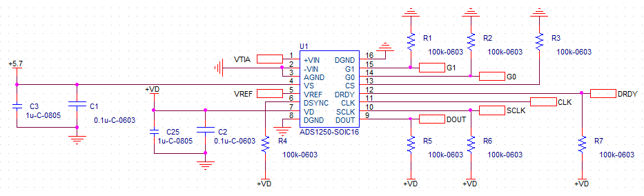
in this project I'm using the ADS1250 to digitize the analog signal;

the power supply architecture is following described:

there is a master power line coming from a switching regulator that give 12V;

the input of a TPS7A4901 is connected to the master 12V and the output of this ldo is 11V; the output of the TPS7A4901 that give 11V is connected to the input of another TPS4901 to reach 5.7V;

+VD is given by a MC78L05ACD with the input connected to the master 12V;

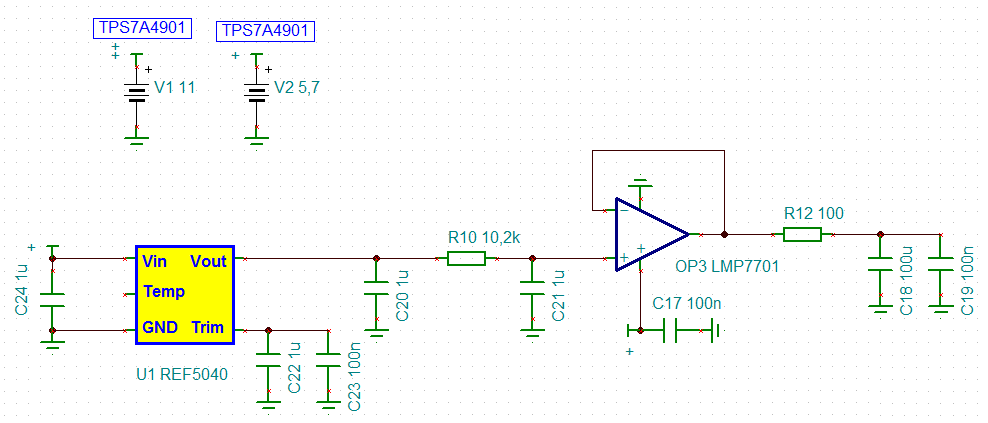
to give the reference to the ADS1250, I'm using the following circuit:

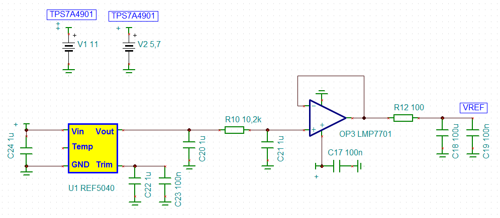
all the capacitor is MLCC, the 100uF on the LMP7701's output is tantalum capacitor;

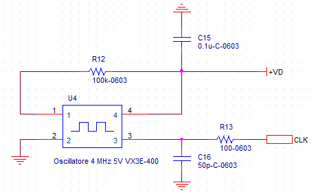
the ADC's clock frequency is 4 MHz;


ADC, clock, reference and power supply is on the same board and an heavy ground plane is used to distribute the ground in the board;

AGND and DGN of the ADS1250 is connected together with a wide copper area in the top layer and this copper area is conected to the ground plane with a via hole

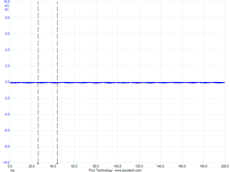
if I measure the FFT of VREF on C19 with the clock signal disconnected to the ADS1250 I obtain the following graph:


if I measure the FFT of VREF on C19 with the clock signal connected to the ADS1250 I obtain the following graph:

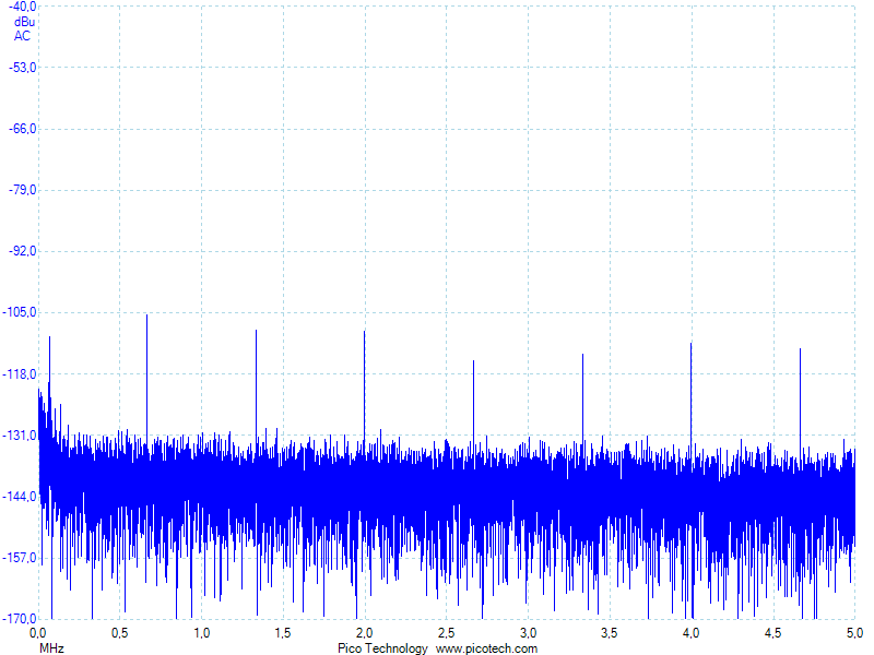
As can be seen from the graphs, a lot of different harmonic components appear when I connect the clock signal to the ADC;

have someone ever seen this behavior before?

I would like to kill this spurious signal because I have to reach the lowest noise level possible;

someone have the solution?

thank you in advance for the answers;

if I have forget something, please, don't exitate to ask me;

Fabrizio 


  • Fabrizio,

    Once you turn on the CLK, the reference is being sampled at the modulator rate.  You will see a transient as the device draws charge, and the reference replenishes.  It is difficult to say if this is really a concern at these levels.  The best possible performance will be with the inputs shorted at mid-supply.  This will show the best the converter can achieve.  If you can achieve the levels of performance shown in the datasheet, then the reference is ok.

    I do have a little concern with the analog supply at 5.7V.  It really should not exceed the specified value of 5.25V.  Absolute maximum is 6V.  This allows for a transient of up to 0.75V above the supply.  This gets reduced when raising the supply voltage higher.  There is really no advantage in doing this with respect to the dataconverter, as the reference is 4.096V which is the highest voltage that can be measured.

    Best regards,

    Bob B

  • Thank you very much for your absolute helpful answer Mr. Benjamin,

    I have some other questions:

    1) Do you think that is possible to reduce the transient in reference output due to ADC charge drawing using a reference buffer with higher output current capability?

    2) Can you explain me better which kind of test I have to perform to evaluate the ADC performance?

    - In more datail:

    a) which kind of DC input stimulus I have to use? I think a really noise free signal such as another reference output signal;

    b) which kind of output parameters I have to check to evaluate the performances of the ADC?

    3) I have to reach 18 bits of final resolution and my AFE can ensure this resolution; do you have any advice to improve the ADC and reference block that, at the moment, is the critical blocks of the chain?


    thank you very much for kindness and for your quick answer


    Best regards


    Fabrizio

  • Fabrizio,

    You are very concerned about the high frequency reference noise, and more than likely this will not be seen.  What you may see is aliasing that may fold back relative to the modulator rate that will not be filtered out by the digital sinc filter.  I would highly suspect that you will have a larger issue due to temperature drift and noise as it relates to the analog input.

    Now to your specific questions......

    1.  The transient may be better viewed with an oscilloscope.  What happens is charge is drawn at the reference input, and the op amp/RC combination is not able to replenish the charge quickly enough.  You have to be careful here to make sure that you don't load the op amp to heavily with a cap load that causes instability of the op amp so that it goes into oscillation.

    2. The best performance will be achieved with shorted inputs biased where the inputs are away from the supply rails.  This is usually done with a voltage divider from the analog supply.  You could use 10k ohm resistors in series so that the input is biased at approximately mid-supply.  This is the absolute best case scenario for DC measurement.  You can take a series of samples and analyze the noise.  The ENOB noise peak to peak is ln(FSR/Peak to Peak noise)/ln(2) with FSR and noise in volts. FSR is Full Scale Range.  For the noise peak to peak, you can either look at the code spread and convert to a voltage, or process the data in a spreadsheet and look at the data graphically to see the voltage spread of the noise.

    If you use another reference voltage as the input, you will not know the noise of the conversion process all by itself.  You will see the noise of the input voltage as well as noise from the conversion process.

    3. Layout and components in the analog input path will also effect your results.  You can optimize the conversion process, but greatly degrade the overall system performance with poor layout of the PCB or using low quality resistors and capacitors in the analog input path.

    Best regards,

    Bob B

  • Mr. Benjamin thank you for your help,

    I'm pretty sure that I don't have dc drift in the analog input because I have measured the AFE output with the scope (unfortunatelly at the moment I'm not able to post the picture mensioned; next week I will post it);

    another reason that leads me to say that I don't have DC drift in AFE output is the following:

    I have the possibility to have the scope samples in an excel file to elaborate them;

    I take 850000 samples of the AFE output and I have calculate the standard deviation of the samples;     

    after I divide the 850000 samples in 16 groups composed of 53125 samples each;

    after I calculate the average of the 53125 samples for each group;

    after I calculate the standard deviation of the 16 averages obtained;

    the standard deviation of the 16 averages, is exactly 4 times less then the standard deviation of the 850000 samples;

    this behavior shows that the 850000 samples, have a gaussian distribution like white noise; if I had some dc drift, averaging the samples, would not have given an improvement like that;

    is this reasoning right?  

    I have a question about point 2: if I take the mid supply voltage from the analog supply with a divider I have at the ADC input a very noisy signal, much noisier than the ADC...how can measure the ADC performance feeding the input with a noisy signal?

    Best regards

    Fabrizio


  • Fabrizio,

    If the signal is common to both inputs, the difference is zero and common mode rejection is quite good with this part.

    Best regards,

    Bob B

  • Bob,

    the AFE output is single ended: the +Vin pin of the ADS1250 is directly connected to the AFE output and the -Vin pin of the ADS1250 is directly connected to GND; 

    my AFE take the current of a photodiode and convert it to a single ended DC value ranging from 0 to 4.096 V; 

    the 850000 samples mentioned in the previous post, are taken in a particular condition for the AFE that is the dark condition;

    what I measure is the noise of the AFE and this noise is compatible with the 18 bits that I want (the rms noise measured is 12 uV);

    the problem is the reference that is outside the 18 bits's limits and can limit the overall performances of the system;

    anyhow thank you for your help;

    Best regards,

    Fabrizio

  • Sorry Bob I thought you speak about the AFE, I realized just now that your post was the answer for the question about the ADC+REF noise charaterization!

    thank you...

    best regards...

    Fabrizio