


Below is the schematic in customer's application system. "IN" is the input for a 1MHz signal.
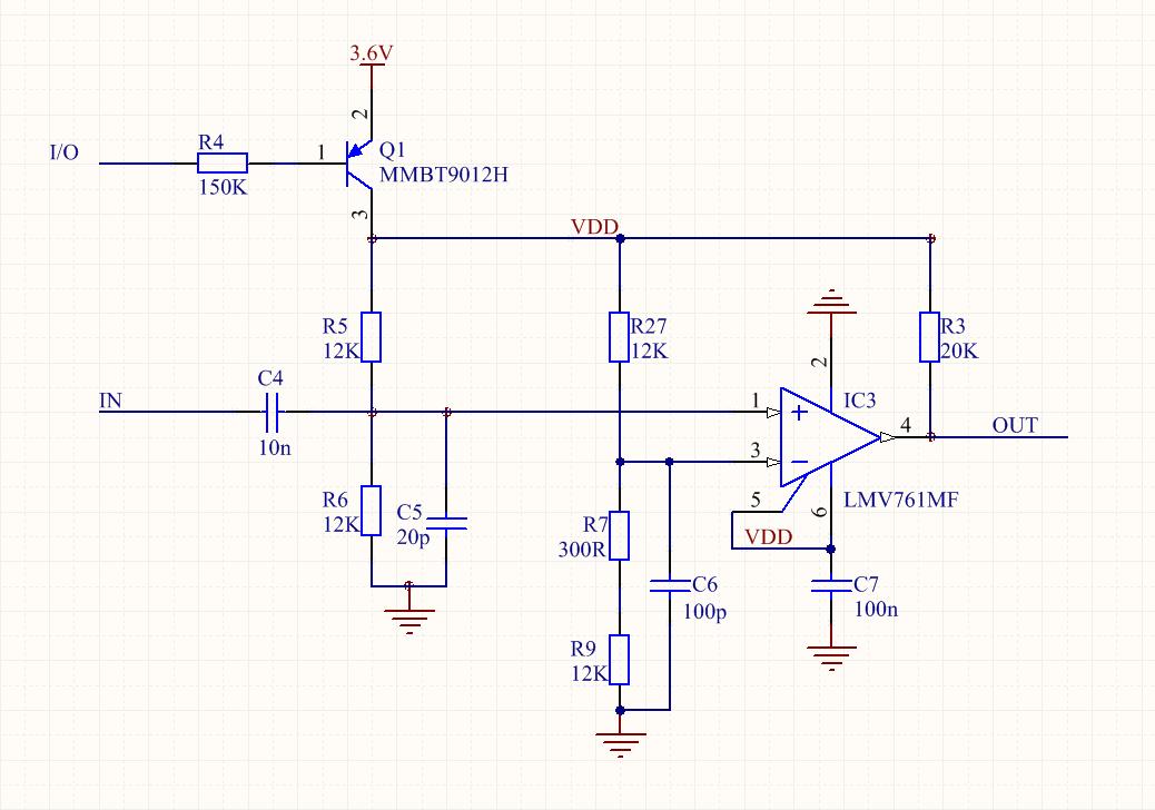
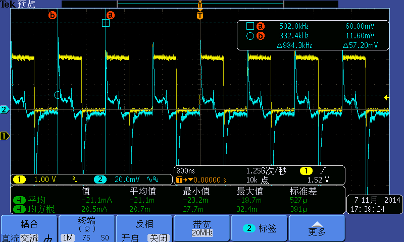
When a 1MHz signal is applied on the "IN" in the front of C4. a same frequency signal is observed on the negative pin(pin 3) of LMV761. below are the test result. why the negative pin is disturbed by the signal on positive pin? where is the transmission path? is it internal or external?\

(CH2 blue signal is on "IN", CH1 yellow signal is observed on pin 3 of LMV761)
(CH1 yellow signal is on "IN", CH2 blue signal is observed on pin 3 of LMV761)
Thanks you
