This thread has been locked.

If you have a related question, please click the "Ask a related question" button in the top right corner. The newly created question will be automatically linked to this question.

PGA2500 defect of daisy chain communication

Other Parts Discussed in Thread: PGA2500, PGA2505

Hello there,

We have a product with eight PGA2500 integrated in daisy chain communication topology.

During the last production batch of 50 products, 5 devices (out of the total of 400) spread over those 50 devices showed a communication problem breaking up the whole chain.

The effect is that SDO of the problematic device is steadily on either +5V or 0V and is fixed to that. When we exchange such a device by a fresh one everything works fine again.

Some of the 5 showed that defect after the first time the product being switched on for prduction test.

What concerns us more is that we have other products which worked fine during production test, where delivered to customers and broke down there.

We do not see them breaking down on the long run (24/7 operation) but have the feeling that it could happen during power-on or power-off.

Could a faulty ramping up of +-5V rails the reason?

What else could be the reason?

Thanks in advance for any comments.

  • Hello Stefan,

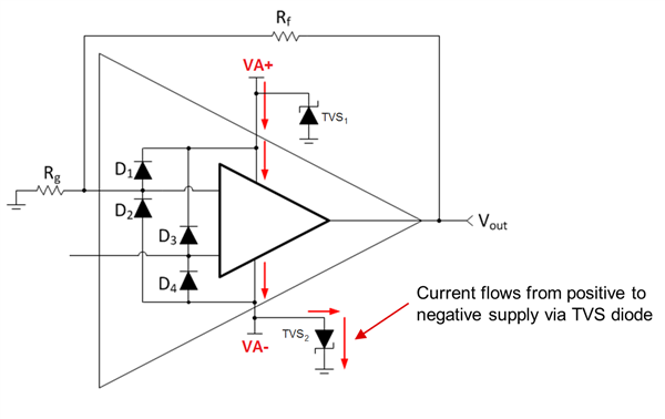
    It is possible to damage a device if one supply turns on before another supply. Please see the TI Precision Lab videos on EOS for information.

    When one supply turns on before another (for example, +5V turns on before the -5V) there may not be a proper current path from the positive to negative supply, so the current finds parasitic paths inside the amplifier which can potentially damage the amplifier. In the TI Precision Lab video on EOS we recommend placing a TVS diode on the power supplies to provide a proper current path if one supply is expected to turn on before another.

    When a communication error occurs does the faulty PGA2500 draw excessive current?

    Is it always the same PGA2500 that gets damaged on the PCB? For example, PGA2500 #3 in the daisy chain configuration is always the one that is damaged but the others operate normally.

    Can you provide a schematic of your design?

    Can you provide oscilloscope shots of your supplies ramping?

    Thank you,

    Tim Claycomb

  • Hello Tim,

    following shows the supplies ramping:

    It is not always the same PGA2500 getting damaged. In the current case it is the first one in the chain.

    The effects of the current defective one and the others in chain are:

    • Defective one: After power up SDO normally is held at GND and ramps to +5V after the first communication has taken place (SDI data, SCLK, CS active) and then keeps at +5V though SDI shows bit activity for setting a gain value.
    • Defective one: After some power ups SDO is +5V directly after voltages ramped up and then SDO keeps at +5V.
    • Defective one: The audio path is functional and lets me input 0 dBu outputting 0 dBu (i.e. 0dB gain seems to be set internally) with THD+N of ~ -100dB which is normal in our design.
    • The next PGA in the chain shows a different gain (+40 dB) and audio path also normal. Gain cannot be set of course because the prior one does not output SDO.
    • All other six PGAs are set to +65 dB gain and audiowise also work normal.
    • Trial of setting gain does not have an effect on the first (defective) PGA2500 and of course also not for the others in the chain.
    • Housing surface temperature of all PGA2500 is similar - no indicator that the first one draws excessive current.

    If the reason for this communication defect could be the voltage ramping: Do you have a precise recommendation for a TVS placement?

    Thank you.

    Stefan.

  • Hello Stefan,

    Tim is out of the office until Wednesday, so I will reply for now.

    Thank you for the new information, including the oscilloscope capture and the description of the failure modes. Please also provide a schematic of your design so we can better assist you. If you're not comfortable posting the schematic here, you may e-mail me at ian@ti.com.

    It looks the supplies are ramping up asymmetrically by several milliseconds. This could be the root cause of the communication failure, and the overall design would benefit from TVS diodes on the power supplies. These should be placed on VA+ and VA-, as shown in the image below from the TI Precision Labs video on EOS. The Vr (reverse standoff voltage) of the TVS should be greater than or equal to 5.25V, the maximum power supply voltage of the PGA2500, such that they can turn on and steer current during power-on or transient events but remain off and in a low leakage state during normal operation. The TPD1E05U06DPYR would be an example of a suitable device.

    Another possible root cause for the issue is the grounding scheme in your PCB layout. The data sheet suggests separate digital and analog planes which connect at a single point, but this can actually cause problems. If the separate ground planes do not have a low-impedance path at both DC and AC, strange biasing conditions could develop at turn on which cause device failures. Based on my experience with this device, I recommend a single ground plane where the traces for the analog signal path and digital communication are kept separate to prevent cross coupling. If you provide your layout, I can review the grounding scheme.

    Finally, any nodes in your system which are exposed to the outside world may require protection circuitry. Figure 7 in the PGA2500 data sheet gives an example input circuit which includes current limiting series resistors and Schottky protection diodes to the rails. If you provide your schematic, I can review this as well.

    Best regards,

    Ian Williams
    Linear Applications Engineer
    Precision Analog - Op Amps

  • Hello Ian,

    I strongly appreciate your support! Thank you.

    I send the schematic sheet of two of the eight mic-ins to your e-mail.

    • The whole system is supplied by a AC/DC SMPS delivering +-5V (and +-15V) connected to central connectors (P1/P2).
    • For each voltage rail and each channel pair we spent in a low-drop linear regulator which supply the analogue chips
    • The oscilloscope capture has been taken from the PGA2500 +-5V  supply pins (i.e. +-4.8V)
    • Directly at the central supply connectors (P1/P2) there are no TVS but instead Shottkys (LSM115J)
    • For each channel pair at the low-drop linear regulators´ outputs there again are no TVS but instead Shottkys (BAT42 at +5V and DFLS130 at -5V)
    • In the layout AGND and DGND are not connected to seperate planes; instead both are connected to GND copper on top (component side), internal GND plane and bottom GND copper

    We are looking for ways to

    a) make the current design 100% robust against normal operation PGA2500 communication failures

    and as a next step

    b) simplify the design for a possibly re-design (where we think about integrating the PGA2505)

    Best regards,

    Stefan

  • Hi Stefan,

    Ian has provided me with the information you sent him. I will review your schematic and get back with you as soon as possible.

    Thank you,

    Tim Claycomb

  • Hello Stefan,

    I have reviewed your schematic and didn't see any issues.

    After looking at the oscilloscope image you provided of the power supplies ramping, it appears that the negative power supply only reaches approximately -4.4V. Can you verify the negative supply voltage (VD- and VA-) at the pins of the PGA2500?

    The PGA2500 requires a minimum of -4.75V connected to VD- and VA-. So if the negative supply voltage does not reach the minimum value, this may explain why there are some communication issues.

  • Hi Tim,

    Yes, VD- is not well below -4.75V - but it´s lower than -4-4V readable from the oscilloscope image when measuring with a DMM.

    But:

    I made some more measurements and found out that the +5V regulator (U4_3) seemed not to work - it showed a voltage drop of only 15mV, i.e. an output voltage of +5.07V from an input voltage of +5.085V. I exchanged it and now it outputs +4.865V what is in the expected range.

    Then:

    I measured between a) Pins 6 (DGND) and 14 (VD-) and b) Pins 6 (DGND) and 15 (VA-)

    • 1st PGA in chain: a) -4.716V (Power-Up) -> -4.684V (after first SDI-data) b) -4.723V (VA+ = 4.865V, SDO = 4.865V after Power-Up)
    • 2nd PGA: a) 4.716V (continous) b) -4.723V (continous) (SDO = -0.024V)
    • 3rd...8th: all similar to 2nd PGA

    After Power-Up the 1st PGA shows -4.716V and at the same time its SDO is 4.865V (=VA+). When the first SDI-communication takes place, though SDO does not change, VD slowly (5 sec) increases to -4.684V. Taking the 10 Ohm (R18_3) and the voltage difference between VD- and VA- into account the 1st PGA obviously draws appr 4mA on its VD- after SDI communication. The others seem to draw only 0.7mA.

    Before I replaced the defective voltage regulator I measured after power up that SDO sometimes was ~0V and sometimes ~+5V and if starting with 0V it ended up with +5V after it "saw" the first SDI bits. Now it always shows +5V after power up and never changes.


    1. Even if VD- and VA+ are some mv beyond the recommended lower limits (VD- > -4.75V / VA+ < +4.75V) could this be a reason for a defect? I take into account, that we have other systems (>95%) working fine with similar VD- / VA+ voltage supplies.

    2. Could the defect of the +5V regulator (I mean VA+= +5.07 instead of +4.865V) the reason for a PGA defect?

    3. What is the function of VD- with regard to the communication part of the device?

    4. Do you have a sort of schematics of the PGA internals regarding protection diodes on its supply pins and SDI / SDO pins?

    Thanks.

    Best regards,

    Stefan.

  • Hi Stefan,

    It sounds like the supplies (VA+, VA-, and VD-) are below the minimum supply voltage of +/-4.75V stated in the datasheet. This is likely the cause of the communication issues you are experiencing.

    Please see below for answers to your questions.

    1. Yes, this is most likely the reason for the defect. Not having sufficient supply voltages will not allow the transistors inside the device to bias properly.

    2. Its possible that the regulator caused some issues. If the regulator was outputting +4.865V, which is above the minimum supply voltage for the PGA2500 I would not expect an issue with the PGA2500 positive supply voltage. However, since the regulator seemed to be experiencing some issues its possible those issues effected the PGA2500.

    3. VD- is the digital supply voltage of the device. Having VD- less than the minimum stated in the datasheet may effect digital communication of the devices.

    4. I do not have schematics of the PGA internals. We cannot share the internal schematics of our devices because it is confidential material.

    Please let me know if there is anything else I can help you with.

    Thank you,

    Tim Claycomb

  • Hi Tim,

    ok, thanks for clarifying.

    I suppose 2., i.e. an unknown incidence destroying the +5V regulator, is most likely the reason for the PGA2500 defect.

    We will dig into this a bit deeper to see how to provocate such an effect on other boards.

    One more thing:
    Is there something to be said about the 10 Ohm resistor between VD- and VA-? Why 10 Ohm and not different value?

    Thank you,
    Stefan
  • Hi Stefan,

    The reason the datasheet recommends a 10ohm resistor is likely to provide filtering of the digital supply pin. The 10ohm resistor and 4.7uF and 0.1uF capacitors provide a cut off frequency of approximately 3.3kHz.

    For help in solving the issue with the +5V regulator, I recommend posting a question to the linear regulators forum.

    Please let me know if there is anything else I can help you with.

    Thank you,

    Tim Claycomb