This thread has been locked.

If you have a related question, please click the "Ask a related question" button in the top right corner. The newly created question will be automatically linked to this question.

OPA699: Clamp circuit

Guru 16770 points
Part Number: OPA699
Other Parts Discussed in Thread: OPA857, , LMH6629

Hi

What is the clamping circuit of OPA857?

I can see the figure 38 about internal ESD protection.

Is the meaning of clamping circuit is nearly equal to ESD protection circuit?

I just want to confirm if the figure 18 of OPA699 is represented as clamping circuit or not, because there is no description of "Clamping circuit" in OPA699 datasheet.

If yes, as the same reason, I believe that LMH6629 also has clamping circuit (ESD protection circuit).

BestRegards

  • OPA857:

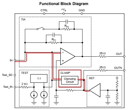
    There are two sets of clamping circuit in OPA857 - a regular ESD diode one (pg 16, fig 38) and the clamp circuit as shown in the functional block diagram on pg 1. The ESD diode circuit steers current to the supplies when voltages higher/lower than supplies occur on the device pins while the clamp circuit between the In (i.e. -Vin of amplifier) and the output of reference is to keep In from going more than 1V above or below the Vref voltage.

    OPA699:

    ESD circuit of Fig 18 is similar to the ESD protection I referred to for OPA857 (not the clamp circuit). This device also has Schottky diode type circuit between the inputs that allows the differential inputs to be up to ±Vs (abs max rating table). If you were curious about the clamps related to VH and VL pins, then they are more sophisticated in their design with some active circuitry to allow linear output till very close to the VH and VL voltages as well as allow the amplifier to come out of saturation quickly if it hit the VH and VL voltages.

    LMH6629:

    This device has regular ESD protection diodes similar to Fig 18 of OPA699 and Fig 38 of OPA857. It also has what is often referred to as back-to-back ESD diodes between the +In and -In to prevent large input differential voltages, hence abs max table has a differential input voltage max of 3V.

    Hope this clarifies the diode protection and the clamp circuit differences between the three devices.

    Thanks,

    Keyur

  • Hi Keyur

    Thank you for your detail information.

    Let me confirm following?

    OPA857:
    The clamp circuit of OPA857 is used not for output clamp but for input clamp. Is it correct?

    LMH6629:
    Does LMH6629 have regular ESD diode and back to back ESD diode individually?
    If yes, What is the difference as usage between regular ESD diode and back to back ESD diode?

    BestRegards
  • OPA857:

    Correct, clamp circuit in below functional block diagram is to keep input from separating too far from Vref voltage, and not intended for output protection. The connection shown between OUTN and Vref is primarily there because OUTN is referenced to Vref.

    LMH6629:

    Yes, it has both. The structure would look something like the below two combined i.e. +/-Vin pins each having the regular ESD diodes as well as the back-to-back diodes between them.

    Regular ESD diodes protect the pins when voltages on these external pins go above or below the supplies. Back-to-back diodes prevent a significant differential voltage from developing between the + and - inputs of the amplifier. In the abs max section of LMH6629 datasheet, you can find a spec that says max differential voltage at 3V. This is the voltage at which the back-to-back diodes will kick in.

    Thanks.

  • Hi Keyur

    Thank you for your reply.

    Regarding to LMH6629, I understood it doesn't have clamp circuit but two type of ESD diode.

    LMH6629 has specification of overload recovery time as 2 nsec.

    Is this recovery time depending on the performance of ESD diodes ? Or only internal transistor performance?
    I'm wondering why LMH6629 has such faster recovery time than that of OPA857.

    BestRegards