Because of the holidays, TI E2E™ design support forum responses will be delayed from Dec. 25 through Jan. 2. Thank you for your patience.

This thread has been locked.

If you have a related question, please click the "Ask a related question" button in the top right corner. The newly created question will be automatically linked to this question.

ONET8551T: chip failure issue consultant

Part Number: ONET8551T

Our current APD-TIA ROSA failure is like this: 

APD-TIA ROSA mounted in transceiver module with power on, the ROSA was damaged when a burst big input optical power (like 0dBm) into ROSA. 

After failure analysis, we found the APD chip breakdown voltage dropped from ~30V to ~14V (breakdown voltage defined at APD dark current equal to 100uA), and TIA Icc is in normal range, but the two output pins (OUT+ and OUT-) common mode voltage difference is big (>0.2V). When inspected under micro-scope, we found obvious damage near the PINA pad of TIA as the following picture showed. We would like to ask:

  1. Is the following picture showed failure from big current? What's the usual TIA failure mode if PINA input current exceeded the limit (4mA)?
  2. About the max input current 4mA in ONET8551T datasheet, is it pick to pick value or average value?
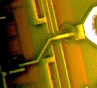
  3.   

We also have other more questions:

3.  Can you explain why ONET8551 operating termperature max limit is 100C? I found other TIA operating temperature is 125C junction temperature.

4. Did TI performed any experiment to prove this parts can only work up to 100C environment temperature (or 105C junction temperature)? 

5. Did TI perform high temperature operating life (HTOL) test on this ONET8551 chip before release? If yes, can you send us the test report? including HTOL test condition, sample size etc.  

5. The following picture is near TIA IN pad  from one failed APD-TIA TO-can, do you think it's damaged from big input current? 


This is urgent for us, please feedback ASAP. Thanks. 

  • Hi Wang,

    To answer your questions:
    1. Is the following picture showed failure from big current? What's the usual TIA failure mode if PINA input current exceeded the limit (4mA)?
    Ans: It is possible that the failure in the picture above is due to applying high current > 4mA at the TIA input pin. The TIA failure mode could be crack (indicating electro-migration) or burns due to metal trace melt (indicating smoke) if the input current exceeded the limit of 4mA.

    2.About the max input current 4mA in ONET8551T datasheet, is it peak to peak value or average value?
    Ans: The max input current of 4mA is an average or DC value.

    3. Can you explain why ONET8551 operating temperature max limit is 100C? I found other TIA operating temperature is 125C junction temperature.
    Ans: The datasheet says that the ambient operating temperature (Ta) max limit is 100'C and not the junction temperature (Tj). As noted in the absolute maximum rating of the datasheet, the maximum junction temperature (Tj) could be 125'C.

    4. Did TI performed any experiment to prove this parts can only work up to 100C environment temperature (or 105C junction temperature)?
    Ans: Please look at answer to question 3.

    5. Did TI perform high temperature operating life (HTOL) test on this ONET8551 chip before release? If yes, can you send us the test
    report? including HTOL test condition, sample size etc.
    Ans: Yes, TI does perform HTOL test on the ONET8551 chip before release. The operating conditions are generally, the DUT supply is max operating voltage and the DUT is in an oven at 125'C for 1000 hours. I am not really sure as why the ONET8551T has any burn-in failures after we have tested for HTOL. Unfortunately, the ONET8551 chip was with a different group and during transition, some of the reliability data went missing due to which we cannot present a test report at the moment.

    6. The following picture is near TIA IN pad from one failed APD-TIA TO-can, do you think it's damaged from big input current?
    Ans: I definitely think that the TIA input is damaged from big input current if it exceeds the maximum average current of 4mA.

    Best Regards,
    Rohit
  • Hi Rohit,

    Thanks for your reply. I have some further questions about item #3, #5, and #6. Please help answer.

    1. Is the following picture showed failure from big current? What's the usual TIA failure mode if PINA input current exceeded the limit (4mA)?
    Ans: It is possible that the failure in the picture above is due to applying high current > 4mA at the TIA input pin. The TIA failure mode could be crack (indicating electro-migration) or burns due to metal trace melt (indicating smoke) if the input current exceeded the limit of 4mA.
    Q: OK, noted.

    2.About the max input current 4mA in ONET8551T datasheet, is it peak to peak value or average value?
    Ans: The max input current of 4mA is an average or DC value.
    Q: OK

    3. Can you explain why ONET8551 operating temperature max limit is 100C? I found other TIA operating temperature is 125C junction temperature.
    Ans: The datasheet says that the ambient operating temperature (Ta) max limit is 100'C and not the junction temperature (Tj). As noted in the absolute maximum rating of the datasheet, the maximum junction temperature (Tj) could be 125'C.
    Q: I noted that the maximum Tj is 125C, but the datasheet recommended operating condition maximum Tj is 105C. But other suppliers' like Semtech 10G TIA datasheet recommended operating max Tj is 125C. I don't know why TI has this difference from others. Currently, we burn-in our APD-TIA TO-can components under 100C ambience temperature, and suffered more than 0.25% TIA failure rate after burn-in. We need TI explain why so high failure rate happened.

    4. Did TI performed any experiment to prove this parts can only work up to 100C environment temperature (or 105C junction temperature)?
    Ans: Please look at answer to question 3.
    Q: OK.

    5. Did TI perform high temperature operating life (HTOL) test on this ONET8551 chip before release? If yes, can you send us the test
    report? including HTOL test condition, sample size etc.
    Ans: Yes, TI does perform HTOL test on the ONET8551 chip before release. The operating conditions are generally, the DUT supply is max operating voltage and the DUT is in an oven at 125'C for 1000 hours. I am not really sure as why the ONET8551T has any burn-in failures after we have tested for HTOL. Unfortunately, the ONET8551 chip was with a different group and during transition, some of the reliability data went missing due to which we cannot present a test report at the moment.
    Q: It's not reasonable for TI such big company that reliablity test report can go missing. I can not accept such explanation. Please help find the report and send to us.

    6. The following picture is near TIA IN pad from one failed APD-TIA TO-can, do you think it's damaged from big input current?
    Ans: I definitely think that the TIA input is damaged from big input current if it exceeds the maximum average current of 4mA.
    Q: we suffered another failure phenomenon is Icc normal, but OUTP and OUTN common mode voltage difference changes big (such as >0.5V), and the sensitivity no good. can you explain this failure mode? and is there a spec about the OUTP and OUTN common mode voltage difference?
  • Hi Wang,

    A clarification in the ambient temperature spec is that the datasheet specifies the maximum recommended operating temperature rating as 100'C to be the "back side operating die temperature". This is not the same as the free-air operating ambient temperature of 100'C, and refers to the temperature recorded adjacent to the TIA die on the ROSA. For the back side operating die temperature to reach 100'C, the ambient operating temperature needs to be several degrees cooler. I believe the max operating free air temperature needs to be limited to 85'C max in order to not exceed the back side operating die temperature beyond the 100'C limit. So, if you are doing burn-in of the APD-TIA TO-Can components at 100C ambient temperature, you are bound to suffer some minor fraction of TIA failures.

    I believe you should be able to operate the TIA up to the maximum junction temperature (Tj) of 125'C, as you are automatically going to cross the Tj of 105'C if the operating back side die temperature reaches 100'C. Let me see if I can help find the report and send it to you.

    Did the other failure mechanism happen also during burn-in? Would it be possible for you to briefly explain the input conditions that caused this failure? Does this big common mode voltage difference happen during over-load condition? I don't think there is a direct spec about the OUTP and OUTN common mode voltage difference and it is mainly tied to getting a clean eye diagram that gives a BER of < 1e-12.

    Best Regards,
    Rohit