I am working on a project. The signal detected needs to be amplified by a lock-in amplifier. I want to know if there is an existing solution or already-made package/chip produced by TI. Any help I will very appreciate.
This thread has been locked.
If you have a related question, please click the "Ask a related question" button in the top right corner. The newly created question will be automatically linked to this question.
Thank you for taking care of my question.
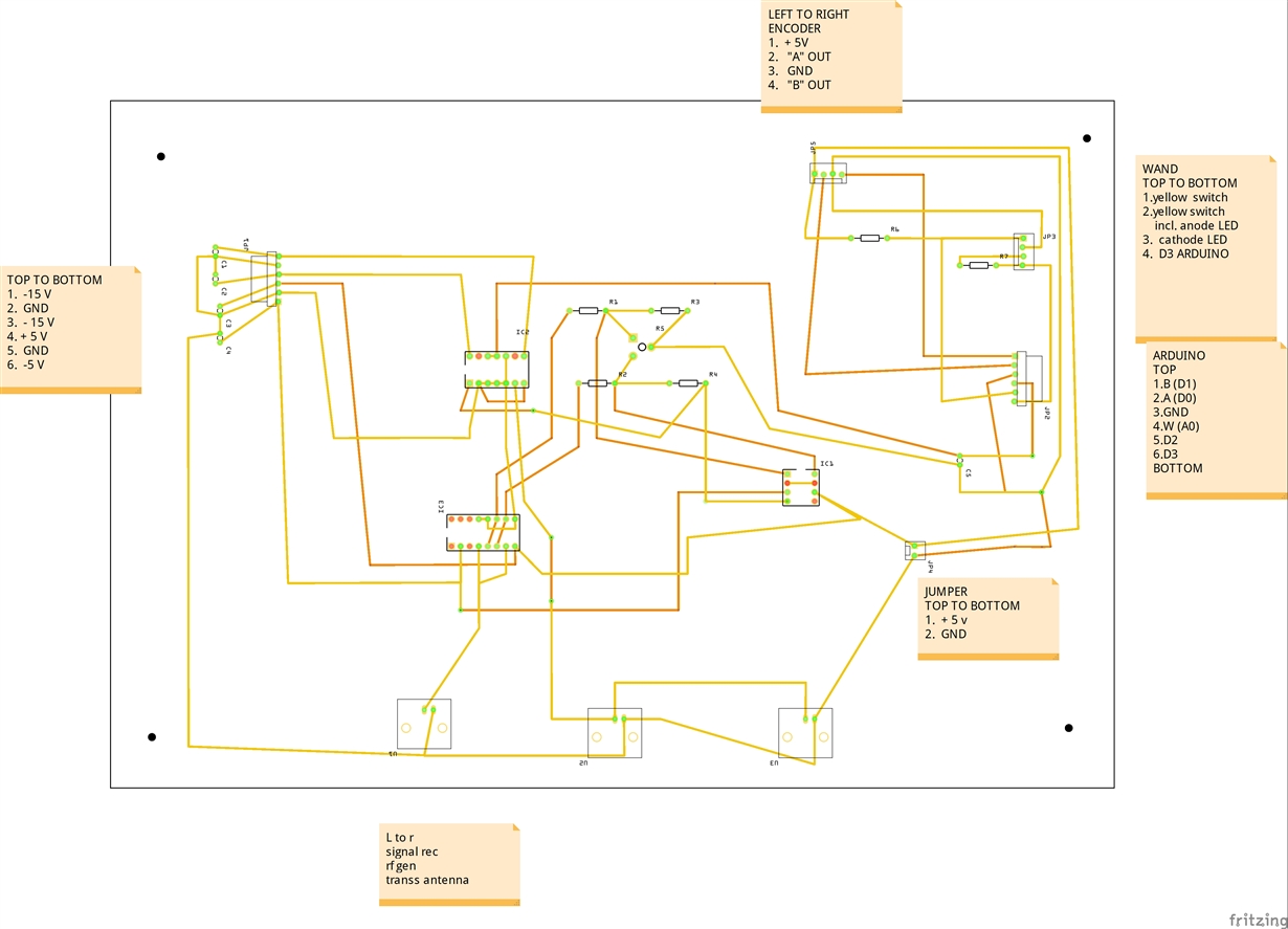
We use a lock-in amplifier to extract a signal with a known carrier wave from an extremely noisy environment. The input is from an antenna which is a kind of detector. We expect the output after passing through the lock-in amplifier can be used as an input of Arduino. I have attached a schematic.
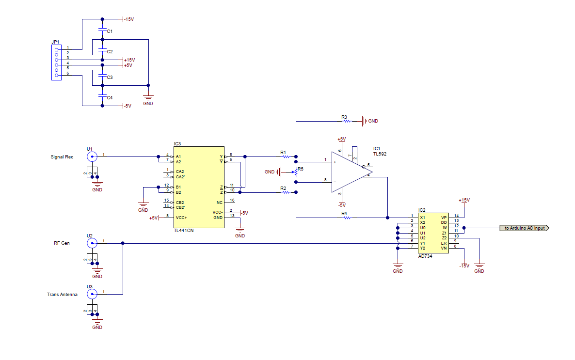
The chip (IC3) with 16 PIN is TL441. The chip (IC1) with 8 PIN is TL592, and the one (IC2) with 14 PIN is AD734.
At the bottom of the board are three BNC connectors. "signal rec" means the signal from the receiver. "rf gen" means the signal from the radio frequency generator. "transs antenna" means the connector to the transmission antenna.
I have populated the board, but the problem is that the signal from the output of the lock-in amplifier mainly is DC, e.g. 4.78V (AC+DC), 0.04 (AC).
Thank you. I will appreciate any help!
Jundong
Hi Jundong,
A layout, as provided, is much less useful than the original schematic would have been. While it took some time, I was able to create the following schematic based off your layout, but component values for resistors and capacitors were not available. If you could provide these, this would help us better analyze your design.
Could you provide oscilloscope images of the signals present at IC3 pin 4, IC3 pin 5, IC3 pin 6, and IC1 pin 4? This would help us troubleshoot what the problem may be. An AC voltmeter reading will not work for these measurements. If it's not clear in the oscilloscope image, please also provide DC levels at each of these nodes.
I'd recommend redoing your PCB layout. While it may work at low frequencies, I would not expect good performance above a few MHz at most. A solid ground plane on the bottom layer, combined with shorter, more direct connections between components will significantly improve your circuit's performance, and reduce PCB size (and cost). In particular, your traces between R1/R3/IC1 pin 1 and R2/R4/IC1 pin 5 should be kept as short as possible to avoid stability issues.
As drawn right now, your layout places decoupling capacitors C1-C4 far away from any of the active components. Combined with the long trace lengths, this may cause unpredictable behavior or degraded performance. Decoupling capacitors should always be placed as close as possible to each active device, with dedicated capacitors for each active device.