This thread has been locked.

If you have a related question, please click the "Ask a related question" button in the top right corner. The newly created question will be automatically linked to this question.

LM1815: Default one-shot timing

Part Number: LM1815

Hi,

I am referring to LM1815 Rev F of the datasheet found here.

If I connect pin 14 to ground, will it disable the one-shot trigger shown in Figure 17?  And the output at pin 12 will align to negative and positive going VR input signals? pin 12 output pulse width will vary based on the frequency of the VR input?

If I connect pin 14 to R, C as shown in Figure 17, will it then enable the one-shot trigger? In this case, will the output at pin 12 align to negative going VR input signal and exhibit a pulse with set by equation 2? and pulse width will not change with frequency of the VR input?

thanks.

  • Howdy Ragulan,

    And welcome to the e2e forums! Yes, you are correct , page 9 of the DS explains that the one-shot can be disabled if pin 14 is directly tied to Ground.

    However, the oneshot controls the pulse width of the reference pulse output, an illustration of this is shown in Figure 18. May I know the application and what you are trying to achieve?

    Best Regards,
    Matt
  • Hi Matt,

    thank you for your reply.

    My application will be an internal combustion engine. LM1815 will be used to interface a Crank and Cam variable reluctance sensors to the microcontroller to calculate engine timing for ignition and injection.

    Here are some additional questions.

    1. Do you have any information on end of life for LM1815?

    2. Do I have to implement the one-shot RC circuit on pin14 to obtain correct negative going zero crossing detection output at pin 10? Or pin 10 will work regardless of RC connection or grounding of pin14?

    3. Why pin12 and pin 10 positive going edges are not aligned in the attached oscilloscope screen capture. I expected them to be aligned?

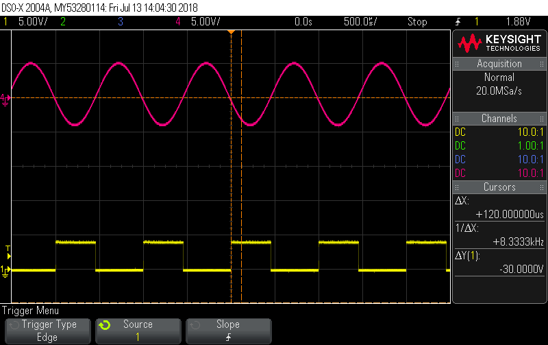
    Details for questions 3 above: I have implemented the attached circuit. I see a phase shift between the input signal negative going zero crossing and pin 12 and pin 10 outputs. Please see the attached oscilloscope capture. Channel 4 is a 1kHz sinusoidal signal connected to "VR SPD IN". It is generated form a function generator. Channel 2 is pin 12 output.Channel 1 is pin 10 output. There may be a phase shift introduced by C303. But I expected pin12 and pin10 output positive going edges to align - not have a phase shift. Please explain what is causing this and how to correct it.

    Thanks,

    Ragulan


  • Hi Ragulan,

    I apologize for the late reply, it seems as though my inbox rules overlooked this post. I'll forward you questions within our team and will provide answers once I receive feedback. If you have any other questions please feel free to update the post.

    Thanks again and Best Regards,
    Matt

  • Hi Matt, thank you for the reply.

    I cannot seem to find the datasheet for LM1815 at the TI website any more. What happened?

    Is this part getting discontinued?

    Do you have any End of life information for this part?

    Thanks,
    Ragulan
  • Hi Ragulan,

    The part is still shown active on it's respective product tool folder: www.ti.com/.../LM1815

    You can disable the one-shot and set pin 10 for Zero crossing by connecting the RC terminal to GND. Additionally the delay you are noticing is mostly created from the internal charging and discharging of the gated structures that are between pin 12 and pin 10. These gates are shown in the block diagram of the device.

    Best Regards,
    Matt
  • Hi Matt,

    1. If the delay is caused by the gate(s), I expect pin 12 to lead pin 10. 900us delay between the edges seem excessive for the gates from pin12 to pin 10
    2. I also expected pin 12 positive going edge to align with pin3 input signal negative going zero crossing preciously, since this edge will be used for engine position determination and subsequent spark and direct-injection (DI) timing.

    Thanks,
    Ragulan
  • Hi Ragulan,

    Did you try the previous suggestions of grounding pin 14 to enable zero crossing at pin 10? As the schematic above shows pin 14 connected to a RC network.

    Best Regards,
    Matt
  • Hi Matt,

    I did try that. It made no difference in signal out at pin10 with respect to input at pin 3.

    Regards,

    Ragulan

  • Hi Ragulan,

    I apologize for the delayed response as I was out during the holidays. I'll need to check within our group to verify these functionality cases. You mentioned that the above experiment didn't have any impact on the output, would you be able to share the oscilloscope capture for the experiment?

    Best Regards,
    Matt
  • Hi Matt,

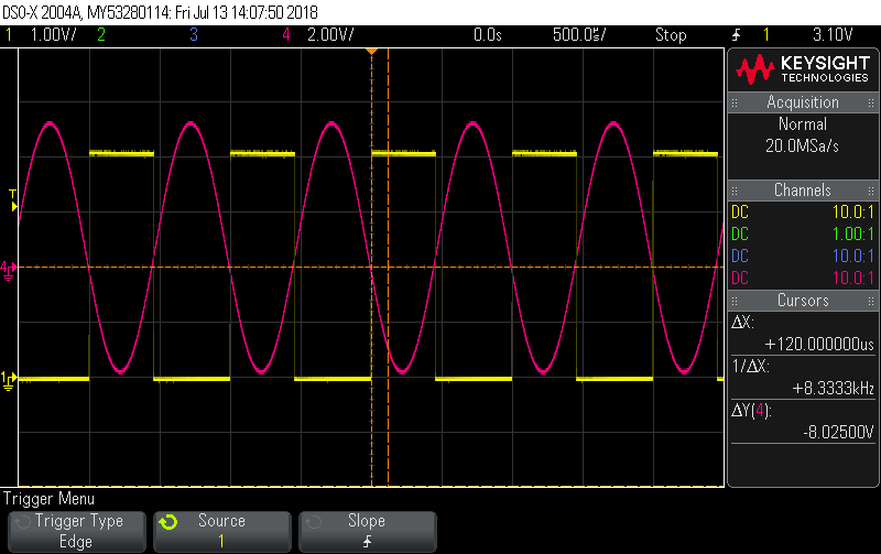
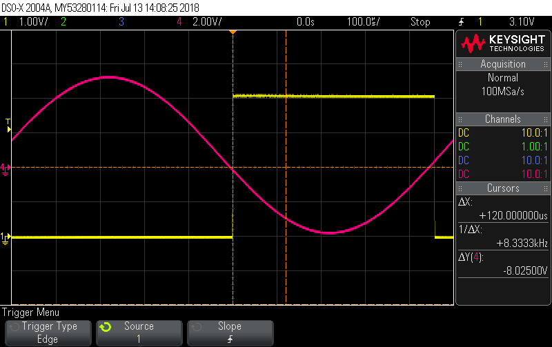
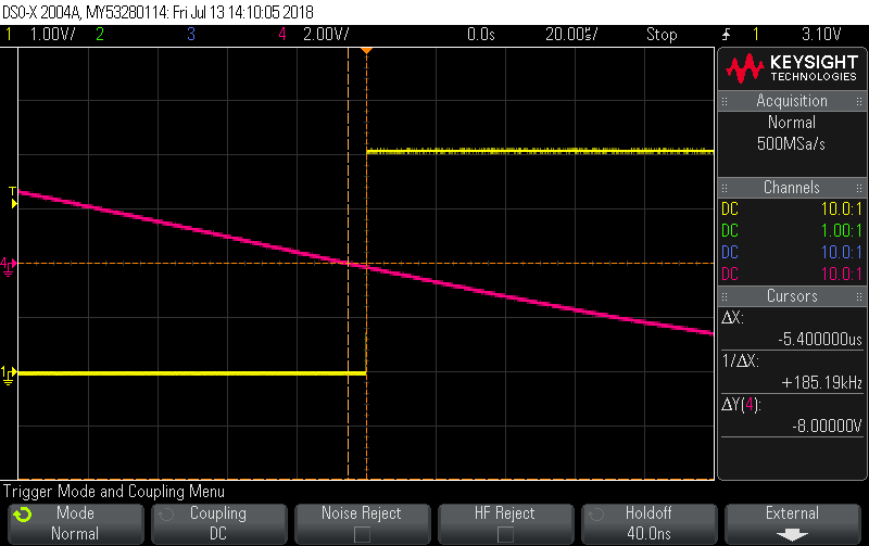
    I tried again with Pin14 grounded. Now the output signal positive going edge seem to align with input signal negative going zero crossing as I expected with little delay (5.4us). I have attached some screenshots progressively zoomed-in to show the zero crossing.

    Thanks for your support.

    Regards,

    Ragulan

  • Howdy Ragulan,

    That is great news, I'm glad you were able to resolve the issue.

    Best Regards,

    Matt