This thread has been locked.

If you have a related question, please click the "Ask a related question" button in the top right corner. The newly created question will be automatically linked to this question.

[FAQ] INA190: How Offset (Vos) and Bias Currents (IB) Affect Low Current Measurements

Part Number: INA190
Other Parts Discussed in Thread: INA240, INA138, INA216, INA270, INA193, INA203, INA200, INA226, INA170, LMP8645, INA223, INA282, INA210, INA199-Q1, INA180, INA181, INA121

What are the design considerations when making small current measurements? How do we analyze this error especially for offset and bias currents of the current sense amplifier?

  • There are several error sources to consider when sensing current (or using amplifiers in general) such as CMR, PSR, noise, gain error, and voltage offset drift, but two device properties (input bias current (IB) and input offset voltage (VOS) ) are critical for DC accuracy, especially in low-current applications. Of these two error sources, the dominant error source is usually IB for using current-shunt monitors (CSMs) in low-current applications*.

    *This is NOT the case for the extremely low IB (0.5 pA typical), INA190, which is very different and more precise than most CSMs. If you need to measure very low currents (µA to mA) with high accuracy please consider the INA190.

    Consider Error from Vos

    • Limits the minimum measurable VSHUNT
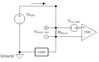
    • Vos is modeled as positive voltage source at the non-inverting terminal.
    • Vos in datasheet is usually characterized by shorting inputs together (VSENSE = 0) and measuring output.
    • % Error from VoseVos = Vos_max/Vshunt_min × 100             (Equation 1)

    Figure 1: Typical High-Side Current Sensing Application with Vos of CSM Modeled

    Keep in mind, the Vos will vary additionally with the common-mode voltage (Vcm) due to CMR limitations. Vcm is defined as the average voltage common to both input pins, but for this analysis is approximately VBUS since shunt voltages are small. You can learn how to calculate this error in a complete error analysis seen in the following reference design as an example or of course with our current sense amplifier training video series.

    Overall, the higher the Vos, the higher your VSHUNT_MIN will have to be in order to meet an error requirement for some minimum current. Which means you could either increase RSHUNT, (despite cost, power dissipation, and board space) or choose a part with lower Vos. Additionally, you can perform a 1-point, system calibration to calibrate out the offset of a specific device. This would require measuring the offset of the device, storing this value in memory, and subtracting out this value when converting your output measurement into a current value. This is possible because the offset for an individual part will remain the same under similar condition (temperature, power, Vcm, etc.)


    Consider Error from IB

    • Directly limits the minimum measurable current (or  ISENSE).
    • Limits the resistor values when implementing an input PI filter. Go here for more info.
    • Along with IQ, contributes to power consumption.
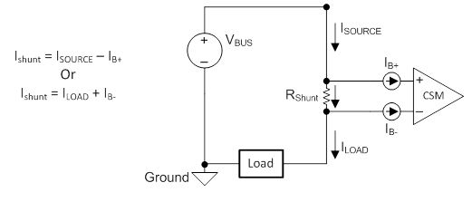
    • IB+ and IB- are modeled as current sources into the amp and IOS is the difference between them.
    • IB in datasheet is usually characterized from shorting inputs together (VSENSE = 0).
    • eIB = I× RSHUNT/VSHUNT_MIN_IDEAL × 100 = IB / ISENSE_MIN × 100           (Equation 2)

    Figure 2: Typical High-Side Current Sensing Application with Ib of CSM Modeled

    While it is easy to calculate the eIb, what current you are actually trying to measure will dictate if you see the measurement higher or lower than what it should be. For example if you are pursuing a high-side scheme as in Figure 2,

    VSHUNT = (ISOURCE - IB+)×RSHUNT  =  (ILOAD + IB-)×RSHUNT

    Thus according to this equation, if IB >0, then your measurement of ISOURCE will be lower than the true ISOURCE value and your measurement of ILOAD will be higher than the true ILOAD value.

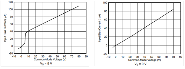
    Similarly to Vos, IB can also vary with Vcm. For example, in the INA240 datasheet the following plots of IB vs. Vcm (see Figure 3) are shown and can shed light on what the designer can expect from the IB for various Vcm, even when part is powered off.

    Figure 3: Most datasheet IB specs are defined when common mode voltage is greater than supply voltage.

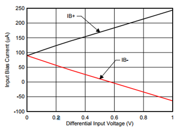
    Also note that IB will change with the input voltage VSHUNT (Vdiff) see INA240’s IB behavior versus Vdiff below in Figure 4. This behavior is mostly dictated by the differential input impedance of the device. At one point IB- can become negative for positive Vdiff, but this will occur outside the dynamic range of the device. 

    Figure 4: How the IB+ and IB- change as VDIFF increases

    Ok finally… let us show how these errors present themselves in a low-current application. Say we wanted to sense high-side current that could range from 250µA to 1mA at a common mode of 12V using the INA240 powered with a 5V supply. 

    Immediately, using Equation 2 we can quickly calculate that IB (90µA typical) alone will contribute to roughly 36% error when sensing 250µA and 9% when sensing 1mA. Assuming this error is acceptable, you might determine the most optimal RSHUNT should be somewhere between 5Ω and 25Ω. Let’s theoretically calculate the numbers using IB values from Figure 4 and for shunt resistors of 5Ω and 25Ω. Results are in Table 1.

    Table 1: Determining error and output voltage for low-current ranges and two different shunt resistor values. Green voltage output means VOUT is in output swing range, red means value is outside output swing range.

    It’s clear that IB is the dominant source of error no matter the RSHUNT value. If you increase RSHUNT, you’ll not only increase VDIFF and thus IB according to Figure 4, but you will begin to lose dynamic range, since your VOUT cannot exceed 5V. If you decrease RSHUNT, eVos will begin to contribute to the total error.


    What to do if we need way less error?


    Alternative 1 – Choose a CSM with lower IB (Hint: INA190)

    The INA240 is better suited for in-line motor control because of its enhanced CMR rejection. Other current sensors are in Table 2. Pay attention to the INA190 which has an IB that is lower than all of the other devices by three orders of magnitude. This is because of its capacitively coupled input stage, which gives it much higher input differential impedance.

    Device

    IB typical (µA)

    INA190

    ±0.0005

    INA138/168

    2

    INA216

    3

    INA270

    ±8

    INA193,4,5,6,7,8

    ±8

    INA203

    ±9

    INA200

    ±9

    INA226

    10

    INA170

    10

    LMP8645

    12

    INA223

    18

    INA282,3,4,5,6

    25

    INA210,1,2,3,4,5

    28

    INA199-Q1

    28

    INA180

    80

    INA181

    75

    INA240

    90

    Table 2: Current Sense Amplifiers Sorted According to Typical IB

    Please also look at the low-current measurement designs TI has to offer below.

    TIPD135 - 10uA-100mA, 0.05% Error, High-Side Current Sensing Solution Reference Design

    TIPD156 - Low-Drift Bidirectional Single-Supply Low-Side Current Sensing Reference Design

    TIPD104 - Current Sensing Solution, 10uA-10mA, Low-side, Single Supply

    TIPD129 - 0-1A, Single-Supply, Low-Side, Current Sensing Solution


    Alternative 2 – Implement an Instrumentation Amplifier

    Instrumentation amplifiers (in-amps) might seem to accomplish the same task as current shunt monitors, and they can even have the same device name prefix ‘INA’ e.g., INA240 (a current shunt monitor) and INA121 (an instrumentation amplifier). However their differing internal topologies beget differing advantages.

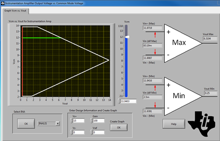
    In-amps do possess very high input impedance, so their bias currents can be extremely low (~pA), but in-amps are constrained to their VCM vs. VOUT curves, which you can calculate here given the supply and gain. On the other hand, CSMs can inherently possess a very large common-mode range. Try substituting an in-amp for the previous example and you will realize it will only work if power supply is >12V (see Figure 5 below), which adds cost, board space, and power consumption. You can download this tool here.

    Figure 5: Showing the rail limitation of an instrumentation amplifier on common mode


    Alternative 3 – Implement a Low-Side Current Sense Scheme with an Operation Amplifier (OPA)

    This would require an amplifier with a true rail-to-rail input (RRI) common-mode range, unless the designer grants this OPA a negative power supply, which would increase cost and board space. While you can certainly choose an RRI amplifier with low IB, low VOS, and a decent GBW, you should in return expect reduced gain accuracy, higher IQ, higher drift, increased board space/cost for external resistors, and a ground potential that is not truly 0 Volts anymore. Additionally, low-side current shunt schemes cannot deterministically distinguish between the system being powered off and a fault condition where bus power supply that you are measuring is shorted to ground. In both scenarios, the OPA will read zero-current conditions (VDIFF = 0V).