This thread has been locked.

If you have a related question, please click the "Ask a related question" button in the top right corner. The newly created question will be automatically linked to this question.

INA826EVM: Gain setting of amplifier.

Part Number: INA826EVM
Other Parts Discussed in Thread: INA826, TINA-TI

Hi,

I have placed Gain resistor on the eval board INA826EVM. But i am not getting output with expected gain. Could some help be please provided if i am doing something not right?

The value i have placed on the eval board:

Gain resistor Rg = 12.4K (Expected gain 5v/v)

Input resistors R1 = R2 = 100R.

Input capacitors C1 = C3 = 100nF; C2 = 1uF.

Output resistor Ro = 100R

Capacitor C0 = 1nF.

Ref shorted to Ground i.e. R5 = 0R.

I am providing input 0.516V dc and expecting output 5*0.516V = 2.58V. But the output i am getting is only 2.27V which signifies gain of 4.29V/V only.

Thanks.

  • Hi Deepti,

    R5 = 0R is not good because this will short circuit the output of U2!

    What supply voltages do you use? Which common mode input voltage does the signal have?

    Have you provided a return path for the input bias currents of INA826?

    It would be the best if you would post a schematic with all the informations needed...

    Kai
  • Hi Kai,
    Thanks for the response.
    U2 is not fitted on the eval board. Hence Vref = 0V is ok.
    +Vs = 10V.
    -Vs = 0V.
    +IN = 0.516V.
    -IN = 0V.
    The input to op-amp is provided by DC power supply.

    I am just using the eval board with values mentioned above. No customised schematic.

    Thank,
    Deepti
  • Deepti,

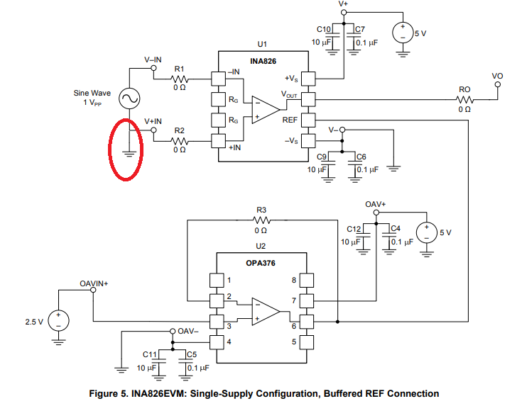
    The fact that U2 is not fitted on the eval board does NOT mean Vref = 0V but rather Vref is floating and this is a worst thing you can do.  Vref MUST be connected to low impedance node capable to sink/source current.  Also, you did not answer Kai's question whether the input differential voltage is referenced to system ground (see in red circle below) or is it floating? Input voltage source must be referenced to sytem ground, which controls the input common-mode voltage as well as provides input bias current to the input differential pair. 

    All in all, picture is worth thousand words, thus please provide the schematic (even hand-drawn) instead of writing a book.

  • Hi Marek,

    Please find the eval board schematic:

    www.ti.com/.../sbou115c.pdf

    Figure 6. And Table 1 for Bill of Materials on default eval board.

    As mentioned before, U2 and other associated components are not fitted on the board. And R5 = 0R is fitted to provide Vref = 0V (system ground).
    The system ground 0V is connected to the following:
    1) -Vs.
    2) -IN (common-mode voltage is 0V.)
    3) Vref.
    4) Ground reference for Vout measurement.

    Thanks,
    Deepti
  • Hi Deepti,

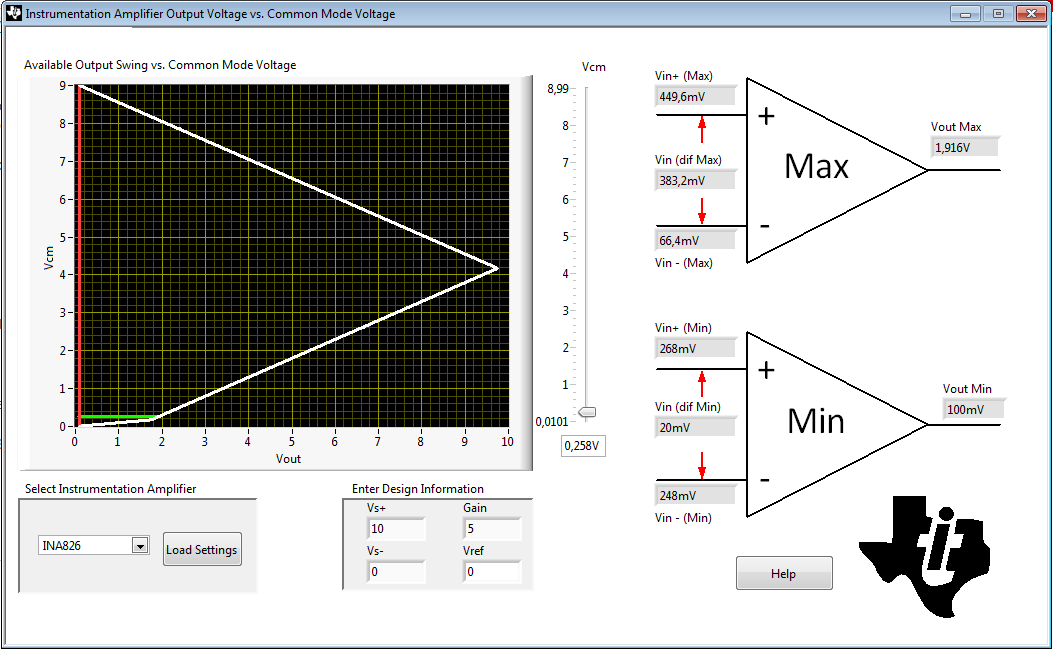
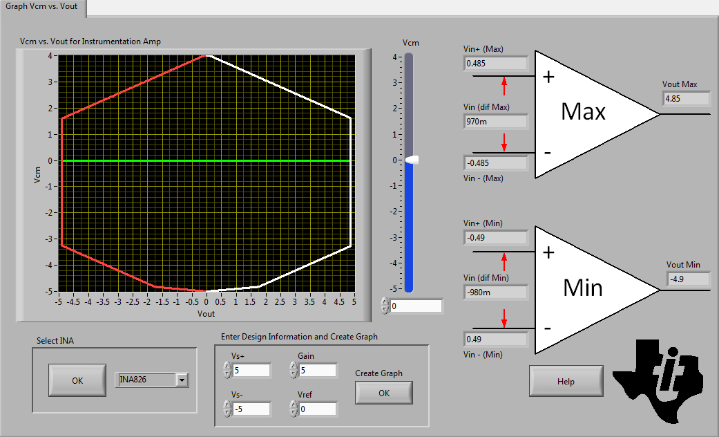
    download the TI's Instrumentation Amplifier calculator to see what input and output voltages are possible with a certain supply voltage and a certain common mode input voltage:

    Kai

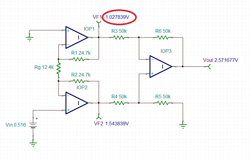
  • The reason behind the result shown above in Kai's reply is that in order for the instrumentation amplifier to process your input signal on a single supply, this would require one of the internal outputs, VF1 (see in red circle below), to swing below negative rail, which is not possible.

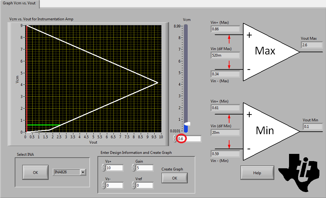
    Therefore, in order to process your input signal you must either lift your input common-mode voltage, Vcm, above 0.6V - see below:

    or use dual supplies as shown below:

    In addition to TI Instrumentation Amplifier Calculator, please download the free Tina-TI available on our website so you may simulate the input/output ranges using attached schematic.

    Deepti INA826.TSC

  • Deepti

    We haven't heard back from you so we assume this answered your questions. If not, just post another reply below.

    Thanks
    Dennis