This thread has been locked.

If you have a related question, please click the "Ask a related question" button in the top right corner. The newly created question will be automatically linked to this question.

LT1013M: Input Offset VS Temperature Graph

Part Number: LT1013M
Other Parts Discussed in Thread: LT1013, LT1013AM, LT1013D

Hello Team,

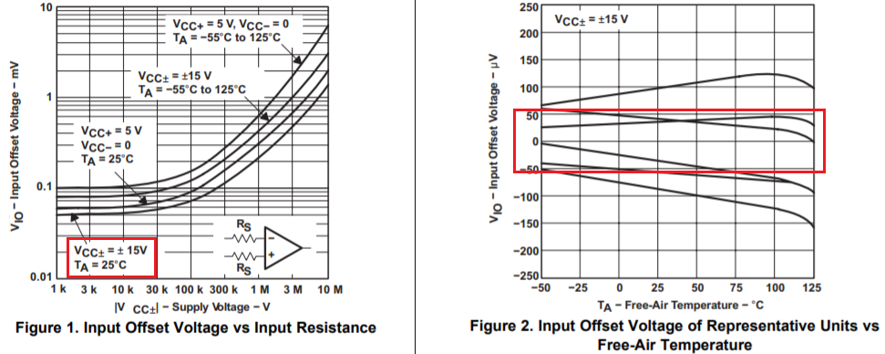
Need your inputs on this. We are looking at Figure 2 on the LT1013x  datasheet. Although there were several curves given, it does not show which device variant defines a particular curve. We tried correlating with the parameter values present in the electrical characteristics table was unable to find the appropriate curve in the graph. Our customer is using the military version LT1013M. Can you guide us on which curve should we reference in checking for the input offset voltage VS temperature characteristics?

Thanks in advance!


Kind Regards,

Jejomar

  • Hi Jejomar,

    these are just six curves of six individual LT1013. They shall show what different temperature drifts can be expected from a LT1013.

    Kai

  • Hi Jejomar,

    I can ask the system engineer, but it may take a few days. 

    The six packages in LT1013 are likely referenced to LT1013C, LT1013D, LT1013DI, LT1013M, LT1013AM and LT1013DM. Among them, LT1013C, LT1013M and LT1013AM have the least input offset voltage at Vcc=+/-15V, Rs < 10kOhm at 25C, Vout=0 presented in the datasheet. 

    LT1013AM has the least input offset voltage variation from the datasheet, which is likely the flat trace inside of red box, see figure 2. 

    LT1013C is likely the last trace inside of red box (only rated from 0-70C). The middle trace in the red box may be LT1013M (not 100% sure). 

    Best,

    Raymond

  • Hi Jejomar,

    LT1013 IC is legacy product. I was told that it may not be possible to track down the information per your request.

    Figure 2 is meant to show the typical changes of  input offset voltage vs. temperature. If you are taking into account of the full temperature range of input offset errors (worst case)  from the datasheet, LT1013M has the lowest input voltage offset errors, which it is likely the one I predict in the previous reply. In other words, even if we are able to label each trace shown in Figure 2, you still have to use the maximum input offset voltage figures per the datasheet in your design requirements (unless you are going to find a way to screen each IC individually from a lot). 

    Best,

    Raymond


  • Legacy indeed, using a 1988 part is perhaps not the best idea, here are some much more recent alternates to consider - not sure any of these are M qualified