This thread has been locked.

If you have a related question, please click the "Ask a related question" button in the top right corner. The newly created question will be automatically linked to this question.

OPA2189: OPA2189 input offset and bias current temperature drift.

Part Number: OPA2189
Other Parts Discussed in Thread: OPA2182, OPA189

Hello,

I require input offset and bias current temperature drift data of opa2189. The information is not given in the datasheet. In my design I use large resistors therefore the bias and offset current drift are important. I tried to extrapolate the drift by looking at the typ. and max. values, but I am not sure how accurate they are going to be.

I calculated 31.66 pA/C of offset drift based on 600pA of offset current(max.) at room 25C and 2.5nA of offset current at 0 from 85 C. (2500pA-600pA)/(85-25). As I said before I don't know if the way I calculated the drift even makes sense. 

Can you provide at least ballpark figures on current drift(offset and bias)? I know that figure 11 kind of shows the bias and offset drift, but it's not obvious what's happening.

Thanks!

  • Hi user5945988,

    The input bias current drift of the OPA2189 will be different for every device and because of that specifying a typical, or ballpark value is difficult. The input bias current (Ib) is a function of the gate current of the input MOSFETs, leakage and charge transfer currents of the chopping switches and leakage of the ESD protection cells, all of which are not correlated with each other. That is why box limits are used for the maximum input bias currents. The exponential increase in Ib seen in datasheet Figure 7-11 is due to the thermally related increase in leakage currents.

    You mention that you are planning on using large value resistors in the OPA2189 circuit. That can sometimes be a problem for chopper/auto-zero op amps. The input currents listed in the datasheet are more representative of an average value. Chopper/auto-zero op amps have chopping switches in the input circuitry, and as they switch there is charge transfer happening between the internal switch nodes. This causes the input bias current to momentarily spike. The spikes are very short in duration but can cause the Ib to be much higher for that duration than when it isn't switching. Large value resistors can result in that currents spikes being translated to voltage spikes at the op amp output and in some cases that voltage noise may be a problem. Additionally, a lack of balance between the inverting and non-inverting sides of the op chopper amp circuit tends to increase the chopping noise.

    If you can show us your circuit, that would help us further asses what you are planning to do and we might have some suggestions for improvements. It may be that a non auto-zero op amp is a better fit for your application.

    Regards, Thomas

    Precision Amplifiers Applications Engineering

  • Hello Thomas,

    Thank you for your response.

    I basically have two different parts of the design that I use OPA2189.

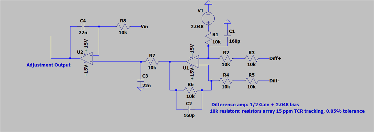
    The first part is basically 3-opamp instrumentation amplifier and the second part is sort of more complicated that consists of a difference amplifier followed by an integrator that is used for DC adjustment. I share the pictures of both circuits along with their input output ranges. All amplifiers are supplied with +/- 15V.

    I am basically trying to figure out what are the major contributors to offset and gain drift. For 3-opamp insturmentation part the major source error for gain drift is gong to be tempco of the resistors (15 pmm as it is stated in the pictures) I don't think opamps' open loop gain is going to come into play because it's too high and doesn't change with temperature. I am now worried about the inputs as you pointed out. This circuit is going into a measurement equipment and insturmentation amplifier's input is going to be connected to the input of the equipment, so switching artifacts are going to be important. As you can see 20pF of capacitance is connected at the input, I assume input current spikes are going to be filtered by those caps is that a valid (or safe) assumption?

    The max. value of reisistance I use 10k, effectively it is 20k at the difference amplifer's input that doesn't seem too large (I changed the design slightly after you mentioned using large resistors can be problematic). Even 100pA/C of offset drift (I assume this assumption is way safer that it needs to be) is going to  result in 2uV/C (Okish for my application) of offset drift and 10pA/C of offset drift would give me 0.2uV/C (way more than enough for my application) of offset drift. I know it's a very crude way to calculate this, but I am just trying understand if I am safe in terms of the offset drift they produce.

    Thanks!

  • Sorry I am using LTSpice :D :D :D 

  • Hello user5945988,

    Well, it looks like you are taking all the precautions needed to minimize the offset drift which appears to be the highest priority in your application. You probably could get away with scaling down all the 10 kilohm resistors by one-half (and doubling the caps) to lower the resistance the input bias currents flow through. That should help with my peak current concerns.

    It doesn't appear you need a great deal of bandwidth in the application. TI has the newer OPA2182, lower power, zero-drift op amp that has a little lower input offset voltage drift of ±0.003 µV/°C (typical) and  ±0.012 µV/°C (maximum), for TA = 0°C to 85°C. That is a bit less than the OPA189.

    Do note that the OPA2182 is only available as dual op amp right now so that might be an issue if you only want to uses singles. Here's a link to the datasheet:

    https://www.ti.com/lit/ds/symlink/opa2182.pdf

    Regards, Thomas

    Precision Amplifiers Applications Engineering