This thread has been locked.

If you have a related question, please click the "Ask a related question" button in the top right corner. The newly created question will be automatically linked to this question.

OPA192: OPA192 As a slew rate limiter

Part Number: OPA192
Other Parts Discussed in Thread: OPA2376

Hello Experts,

I want to design a voltage buffer with a slew rate limiter. I am referring the below document for my design.

Now In this design, I_C1 is considered as 10uA and Saturation voltage as 10mV. where did these values come from? the example shows a design of 20V/Sec.

My requirement is 115KV/Sec. I need an adjustable rise depending on my requirement and cannot use a fixed slew rate opamp. Now when I follow the steps and calculate the values, My circuit is ringing. Can you help me with detailed steps in selecting all the components for the desired slew rate?

Thanks

Vishal

  • Hello Vishal,

    This TI Precision Designs, SR limiter design was released 7 years ago and unfortunately the author is no longer with TI so we are unable to ask him about some of the detailed design decisions. I'll do my best to try and answer for questions.

    The text states, " I_C1 is the current through C1 and will be U1_Vsat/R2. Vout Slew rate is dV/dt=I_C1/C1 by re-arranging the standard capacitor equation of I=C*dV/dt. Regardless of input voltage, slew rate will always be the same." It looks like the author decided to set I_C1 at 10 uA as a reasonable current level. The OPA192 output voltage when very lightly loaded can swing within 5 mV to 15 mV of the supply rail, and the author appears to have settled on 10 mV.

    You mention your design is for a 115 kV/Sec SR limiter. That would be the equivalent of a 115 V/uS slew rate, in which case it is very high slew rate. Is that what you intend? The OPA192 would not be usable for the very fast limiter circuit, but would require a High-Speed op amp instead. The limiter in the TI Precision Design using the OPA192 is for a SR a million times slower (20 V/S) than the OPA192 slew rate of 20 V/us.

    Regards, Thomas

    Precision Amplifiers Applications Engineering

  • Hi Thomas,

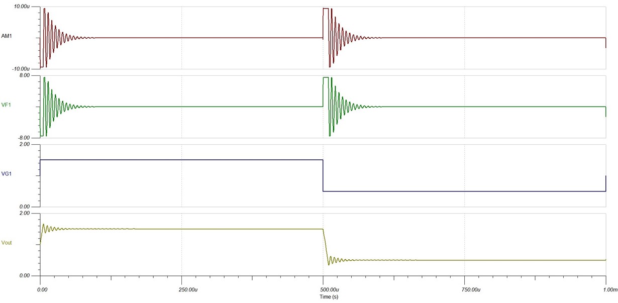
    Sorry My mistake, Me desired slew rate is 115mV/uS.  So My R and C will come 797K and 89pF.  Author says choose a op-amp with slew rate 10 to 100 times  greater than the desired slew rate. so I think OPA192 is ok.  Please check the attached waveform and Simulation file for your reference.

    Slew rate limiter.TSC

    Regards

    Vishal

  • Hi Vishal,

    Please check the following configuration, and it will minimize the oscillation. I did not check your slew rate and bandwidth requirements (assumed this is what you calculated). In theory, I should add another pole (capacitor, say C3, where (C1||C3)*R3) at a higher frequency) above C1 and R3, please see if this is what you want. 

    Best,

    Raymond

  • Vishal,

    Looks like I was off by a few decimal places too! Sorry about that, but now I see you really need 0.115 V/us. Indeed the OPA192 should be suitable for the application.

    It looks like my colleague Raymond has responded with a solution for the ringing. I'll drop back for now.

    Regards, Thomas

    Precision Amplifiers Applications Engineering

  • Hi Raymon/Thomas,

    Thanks for your response. I am trying to simulate the circuit suggested by you, But getting a convergence error after the addition of C2. 

    Regards

    Vishal

  • Hi Vishal,

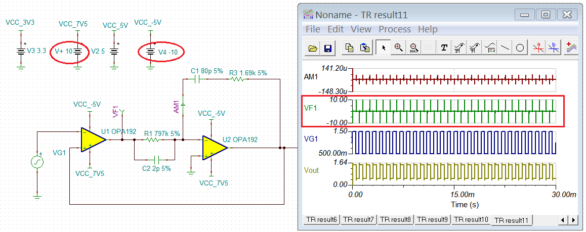
    The circuit has a convergence issue (without adding C2) when you simulate it longer, say 12 msec (selecting Zero initial Values under Transient Analysis). We will take a look why it is. 

    It looks like VF1 node hits rails. Please check the following configuration.

    Best,

    Raymond

  • Hi Raymond,

    How did you arrive at the value of C2 to be 2pF?

    Regards

    Vishal.

  • Hi Vishal,

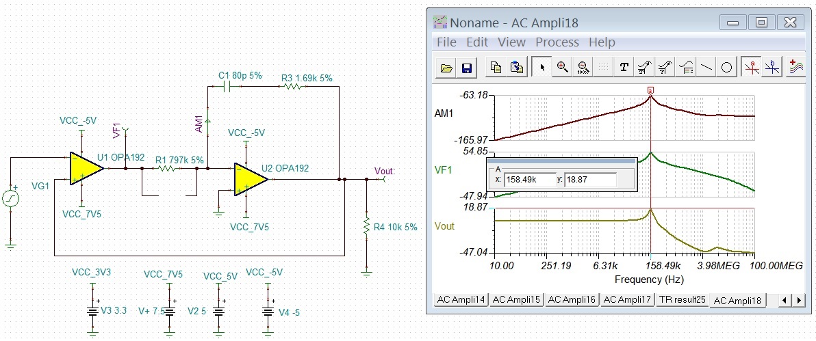
    I did AC analysis in your original circuit, and saw the double poles at approx 158kHz, which is the source of your op amp instability. 

    In order to cancel the pole with a zero, With R1=797kOhm, and C2, I create a zero at approx. 150kHz. C2 was calculated to be 1.3pF. And I modified the value slightly based on the transient and AC analysis.

    There are still some issues with U1, where the gain is too high, which is part of convergence issues. In the real world, output railed out at Vcc and Vee maybe ok, but tool does not like it. I will let you know. I assumed that you are ok with the slew rate limiter you created.

    Best,

    Raymond

  • Hi Vishal,

    Can you provide us with the input and output frequency, amplitude requirements? The slew rate is limited to 115mV/usec. 

    Question: Are you getting the slew rate you wanted?

    Best,

    Raymond 

  • Hi Vishal,

    I found the original slew rate limiter schematic, see below. The design uses different op amp, but it should not be problem. OPA192 has higher BW than OPA2376 and the slew rate is 2V/usec. 

    https://www.ti.com/tool/TIPD140

    /cfs-file/__key/communityserver-discussions-components-files/14/OPA2376-SR-Limiter-SS-Final-115mV-per-usec-10282020.TSC

    I am asking the requirements from the previous reply. This simulation is using single 5V supply rail.  

    Anyway, if you have additional questions, please let us know. 

    Best,

    Raymond

  • Hi Raymond,

    My maximum operating frequency will be 50KHz. And I am looking for an adjustable slew rate of 0.01V/us to 0.2V/us. I am planning to use a digital pot for slew rate adjustment.

    One more thing, Can we increase the value of the capacitor as the board capacitance will come in picture for smaller values of capacitors( pico Fadars).

    Regards

    Vishal

  • Hi Vishal,

    What is the required voltage amplitudes from low to high and vice versa in square wave with the slew rate limit? In the previous simulation, the output is between 0.3V to 1.6V or so. 

    Best,

    Raymond 

  • Hi Vishal,

    I am trying to figure out what you are really asking. 

    With 50kHz squarewave, the period is 20 usec. let us say we have slew rate of 0.2V/usec, 10sec will voltage rise at approx. 0.2V/usec*10usec= 2V. With 0.01V/usec, 10 usec will have voltage rise approx. 0.01V/sec*10usec=0.1V. If we have 2V or 0.1V rise, we do not have square wave + slew rate control (rise and fall). It will be sawtooth waveform. 

    In the application note with slew rate limiter, the frequency is only specified up to 250mHz. Please let me know what are your requirements. 

    Best,

    Raymond


  • Hi Raymond, 

    My frequency of operation will vary depending on the slew rate. Maximum it will go to 50KHz. that time, my slew rate will be 0.2V/uS. So my voltage will go to 2V in 10uS. That's exactly my requirement.

    Operating voltages of Opamp is +-7.5V and My maximum output voltage of Op-Amp is 0V to 5V.

    Regards

    Vishal

  • Hi Vishal,

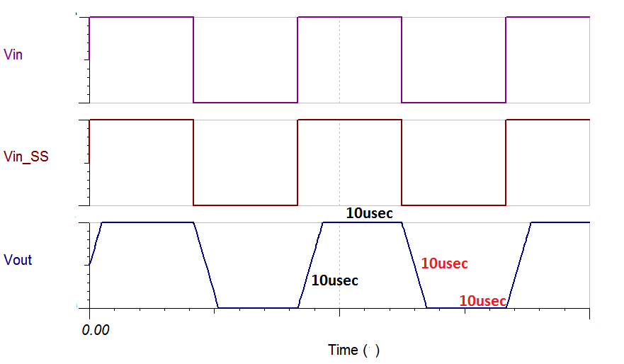
    So you want the output in the following pattern (The waveform on x axis is not proportional scaled). The voltage rise in 10usec is 2V from low to high in 0.2V/usec slew rate. 

    Best,

    Raymond

  • Hi Raymond,

    Yes. That's exactly is my requirement.

    I want to use a pot for slew rate adjustment. How does it affect stability? Is it achievable?

  • Hi Vishal,

    Here is what I have. It is very close, but it is not quite there yet. 

    I swapped the input at U1, and it has better control for high frequency slew rate. The circuit is sensitive with pole and zero in simulation near the corner frequency. I also lowered the rail voltages so that I can manage it better. Please let me know what you think.  

    /cfs-file/__key/communityserver-discussions-components-files/14/OPA192-slew-limiter-new-10302020.TSC

    Best,

    Raymond

  • Hi Raymond,

    This circuit is not working as per my expectations. The output should follow the input. At 2Vpk, The output is saturating close to 1V. My input will usually have a dc Level, with a square wave of +-100mV. at 50kHz.

    Regards

    Vishal

  • Hi Vishal,

    Can I get back to you tomorrow? To control the slew rate at 50kHz may not be easy in this circuit. BTW, the output is not saturating. I lowered the gain with a feedback resistor. 

    Thanks,

    Raymond

  • Hi Raymond,

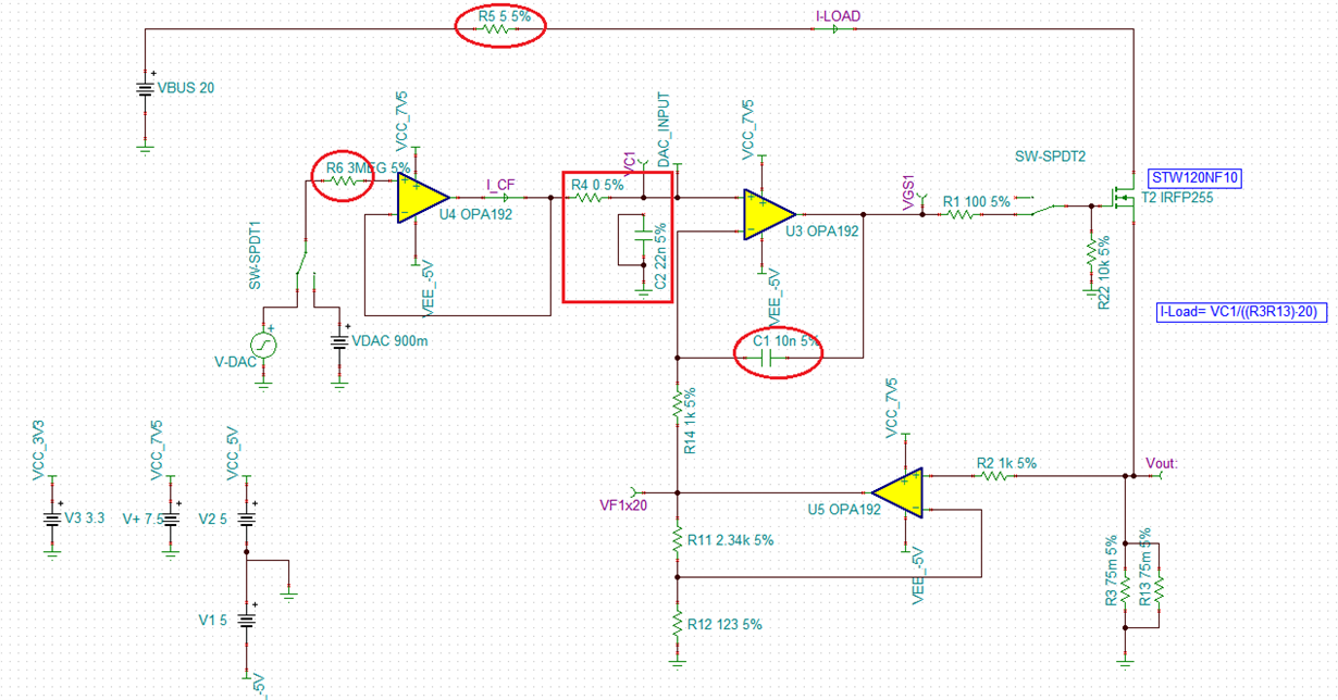
    To give you a full idea, I am designing an Electronic Load for which we have certain requirements for rise time. 

    1. load current should reach the set value in less than 10uS.
    2. Need an adjustable slew rate such as 150mA/uS. (Only when setting current in the beginning).

    I am attaching the Eload Simulation file. Please note the load current is proportional to the input voltage. (Details in the simulation file.)

    Circuit stability: 

    1. In absence of a slew rate limiter, the Current will overshoot.
    2. Currently, its stabilized by R4 and C2. 
    3. But, With R4 and C2, any current will have the same rise time as the RC charging time is the same for all the voltage values.

    And regarding the 50KHz operating frequency, that time A fixed voltage (Set current) with a <10mV square wave input will be given to maintain the load current at a constant value by taking feedback from the ADC.

    So that time, I don't need any slew rate control as it's very fast. Slew rate control is needed only when setting the initial current.

    Eload e2e.TSC

    Regards

    Vishal

  • Hi Vishal,

    I modified some parts of the your circuit. 

    1. Add R5 to limit the current. Your step function is from 1 to 2.5V, which means that the max. current 3.3A. 20V/5 will give you  4A max. Also, it will prevent the overshoot in current.

    2. I reduced C1, the circuit is stable now. It has BW approx. 75kHz with phase margin approx. 74.8 degree. The feedback loop is stable. If the application's operating frequency is 50kHz, you will need high BW in the constant current of the circuit. 

    3. At the input, I added 3MOhm input resistor to retard the BW of the front end buffer. This is not a good way to do it, but I want to see if the current's slew rate is in the application range, and it seems so. If this is ok, I will find a buffer with lower slew rate to substitute OPA192 (slew rate 20V/usec). 

    If the analog front end has a voltage slew rate as you desired, the rest of the circuit should follow, assume the the remaining circuit has the BW to following the input signal. Maybe we will increase the BW on the constant current part of the circuit, and provide a desire voltage ramp in the front end.  

    Please let me know if this is what you have in mind. 

    BTW, is 37.5mohm load fixed? For the low constant current, you can increase the Rsense slightly. Currently, it dissipates approx. 3.3*3.3*37.5mOhm or 0.4W. Also, I do not see a load in your constant current circuit.  

    Best,

    Raymond

  • Hi Raymond,

    • The MOSFET itself is the load. (Entire power is dissipated across the MOSFET.
    • Rsense (37.5m ohm) is fixed. I will set the desired current by adjusting the input voltage.
    • Without using any RC (R4 and C2) circuit, the circuit works well for the rise time of <10uS.
    • In the simulation, it works well for C1-10nF. But actual design needs a min of 22nF capacitor in the feedback.
    • My Entire circuit works well. All I need is the slew rate (Adjustable) control for desired rise times.
    • Instead of input, Can we do something in the feedback path to achieve the desired rise time? Or Any idea on How to select these values? Currently, It's stable with 1k and 22nF (R14 and C1).

    Regards

    Vishal

  • Hi Vishal,

    You have a better way to control the slew rate at 50kHz with the following example. I can try your initial circuit, if you insist, but I am not convinced that it is doable to control it accurately at 50kHz currently. You have to take into account of a stability of the original circuit as well. When I simulated last week, it is very sensitive to poles and zeros in the feedback loop. 

    /cfs-file/__key/communityserver-discussions-components-files/14/OPA192-integrator-11032020.TSC

    Best,

    Raymond

  • Hi Raymond,

    How to stabilize the feedback loop in the Electronic load Circuit? The below link has the same circuit. In order to keep the DAC output smaller and reduce the power dissipation across Rset, I choose a GAIN of 20 in the feedback path. In This document also it's not mentioned how to choose the Riso, CF, and Rfb for compensation. Can you tell me how to calculate these values for stability?

    https://www.ti.com/lit/an/slaa868/slaa868.pdf?ts=1604471367262&ref_url=https%253A%252F%252Fwww.ti.com%252Fproduct%252FDAC80501

    I simulated your circuit for Slew rate, It's not working as per my expectations. Can you suggest something else?

    Regards

    Vishal

  • Hi Vishal,

    As you said, your circuit is stable, except the BW is low for your required 50kHz. However, this circuit is not going to response to 50kHz input step functions. 

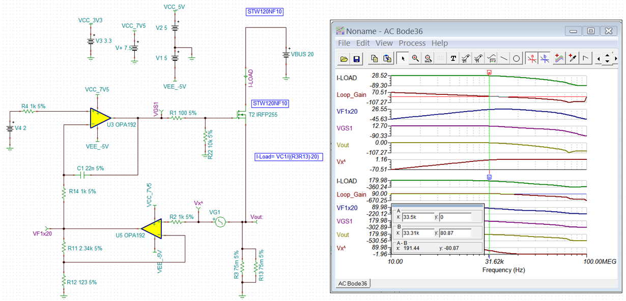
    Enclosed is a method how the loop_gain and stability are analyzed. 

    https://training.ti.com/ti-precision-labs-op-amps-stability-introduction?context=1139747-1139745-14685-1138805-13848

    http://ecee.colorado.edu/~ecen5807/course_material/Lecture14.pdf

    https://www.edn.com/middlebrooks-and-rosenstarks-loop-gain-measurements/

    /cfs-file/__key/communityserver-discussions-components-files/14/Eload-e2e--AC-Analysis-11042020.TSC

    I am enclosing some how to training video and paper on the topic. I provided you with the loop-injection model, and you can determine the effects by changing some of the parameters. 

    Best,

    Raymond

  • Hi Raymond,

    Thanks for your support.

    Regards

    Vishal