This thread has been locked.

If you have a related question, please click the "Ask a related question" button in the top right corner. The newly created question will be automatically linked to this question.

XTR117: Failing ESD Immunity test where TI's TIPD126 design passes

Part Number: XTR117
Other Parts Discussed in Thread: TIPD126, PGA309, STRIKE

Hey everyone,

I am using XTR117 in transmitter product by referring TI's CerTIfied design TIPD126.
We have used same component as shown in the TI's design but we were failing the ESD immunity test. We are going for 8kV contact discharge and 15kV air discharge. We have aluminum enclosure with cut out for LCD display, membrane keypad and external 4-20mA 24V input connector. There is aluminum sensor body attached on the back of the case and sensor wire running the internally to the sensor body and in to the enclosure.

We tested the device with and without protective earth in both case the device failed damaging the XTR117 when disconnected from protective earth LCD was also damaged. When protective earth was connected (also checked that the case's both half and sensor body are connected to earth) no other component was damage apart from XTR117.

As the sensor body and case were connected to earth we hadn't provided any ESD protection devices.

Final device will be used without protective earth.

Q1. Please suggest techniques for ESD protection?

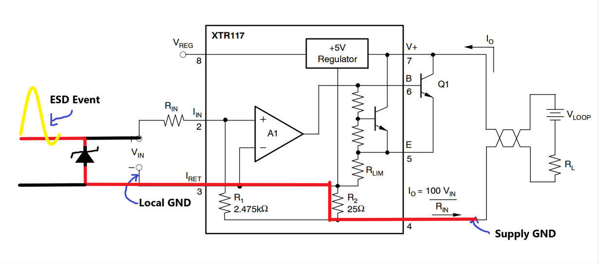
Other concern we have is. When there is ESD event occurs and TVS diode will short it to local GND which is not the supply GND or Earth but the 'local GND' which is connected to the 'supply GND' via XTR117's 25ohm internal resistor.


Q2. Even after adding the requisite protection (TVS Diodes) to the exposed pins will the XTR117 survive the ESD current surge on its Iret pin? Is there anyway to protect the IC?

  • Hi Yash,

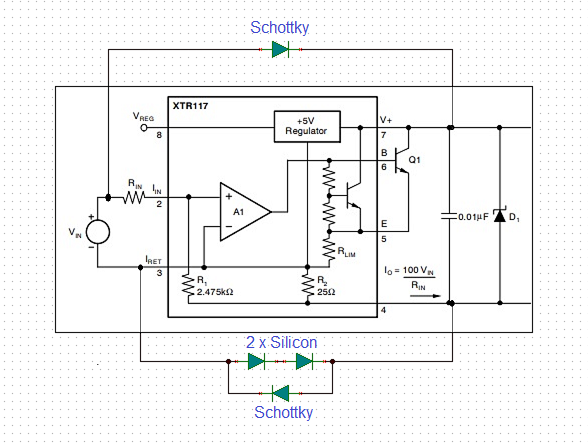
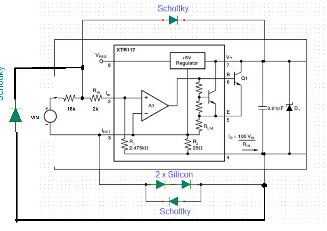
    I would add this protection scheme:

    Kai

  • Hi Yash,

    Are you doing DO-160 Section 22, lightning and Induced Transient Susceptibility Test, also is called Indirect lightning pin injection test? If this is the test, you need to tell us the pin injection waveform class and level for that the particular test. In other words, you need to know the amount of energy will be injected at each pin, and you have to rate the resistor and TVS diode accordingly, and provide a path to discharge the amount of injected energy to earth ground. XTR117 is rated for certain amount of energy to protect itself, it is not designed for pin injection from Indirect lightning test (no IC manufacture does without the specific resistor and TVS protections). 

    For aerospace, ESD discharge test (Sec. 25 of DO-160) does not test connector pins (DO-160 Sec. 25.1), the ESD test is only applicable to an EUT's case (15kV, Cat. A), where any possible human contact locations on the surface of EUT may be tested.

    When subject to 15kV ESD test on an EUT's surface, the EUT has to be ground to earth GND. This class of tests are fairly standard, I think that aerospace, automotive and military ESD test requirements are very similar.

    When performing ESD test, ESD discharge needs to "jumped" to Earth ground when 15kV air discharge is initiated. In other words, you need to provide a low impedance path for the ESD discharge. For instance, if you are performing ESD air discharge near the input's connector of XTR117, and if the connector is made of metallic material and it is in physical contact with EUT's metal enclosure, then XTR117 part should not get damaged (Pin injection at the input of XTR117 is dealt with in Section 22 of DO-160). 

    If the input connector is made of plastic or non-conductive materials, then the outer case of the connector needs to have metallic shields that is required to make direct contact with the EUT's metal enclosure. Otherwise, the EUT is not going to pass this particular test. The ESD 15kV arc has to be discharged immediately via the EUT's metal case. If you allow the high Voltage travels inside of metal enclosure, anything along its paths will be damaged as you have experienced. The 15kV is "looking for" earth ground when arc is initiated, and it will find a  low impedance path to an earth ground until it does. 

    Please let us know if you are performing pin injection or ESD tests.  

    Best,

    Raymond 


  • Hi Yash,

    It looks like in the TIPD126 reference design, the XTR117 input comes from the PGA309. I believe the system level IEC test done in the reference design focuses on external pins. The type of test you are trying to do is important to know as Raymond has explained. However, Kai's recommendation is a good solution for your Q2 as the external diodes will create a current path outside of the device and thus protect the IC. 

  • Hey Raymond,

    Thank you for your informative reply. 

    We are doing IEC 61000-4-2 Level 4 (Contact Discharge 8kV; Air Discharge 15kV).

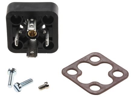
    Also we are using this connector and female connector will be chosen by the customer and we will have no say in it. 

    1. During the first test there was no PE connected to the device and boards were electrically isolated from PE, this caused LCD to fail during the test. 

    2. For second test we connected the PE to both half of the case and the sensor body and boards were electrically isolated from PE, this helped with the LCD but XTR117 failed during contact discharge on the sensor body. As you mention in case of the connector if the connector is connected to the metal case then nothing should get damaged but during contact discharge on the sensor body which is connected to the metal case (I did continuity test) still XTR117 failed. And when the connector is connected there are no expose pins so I assume the ESD will not take the connector route. 

    ESD strike which damaged the XTR117 was done on the metal bolt on the black sensor body. 

    3. We also had battery power source for the same device, where 4-20 mA connection was not there and PE was not connected (both were electrically disconnected). In that case everything worked fine and passed the ESD test.

    *Important thing to note is that the device will be just 2 wire and it will never have a PE, according to standard it is not required for low voltages (24V DC) application, we just tested it when connected to PE, to see what result we would get. Also there was no ESD protecting added for the LCD pins or the membrane keypad pins, planning to add it in our next revision*

    Few key take away I have found with respect to ESD, please correct me if I am wrong, is that the board and the metal enclosure forms a capacitor which protects the board by storing energy from the ESD capacitor and then bleeding the energy slowly. But it is not exactly working for us. So should we add a capacitor between local GND to the enclosure (chassis earth) wherever we have TVS diodes protecting the pins like LCD & keypad pins so the excess energy will not flow through XTR117 or should I also add the diodes arraignment as shown in Kai's earlier reply?

  • Hi Yash,

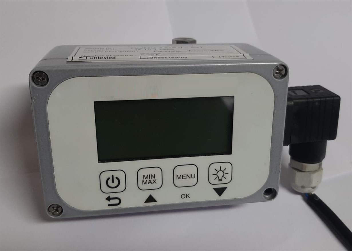
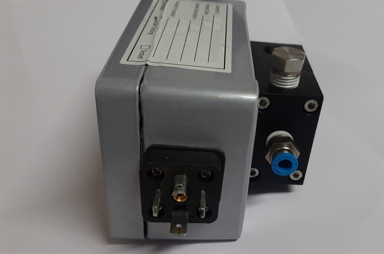
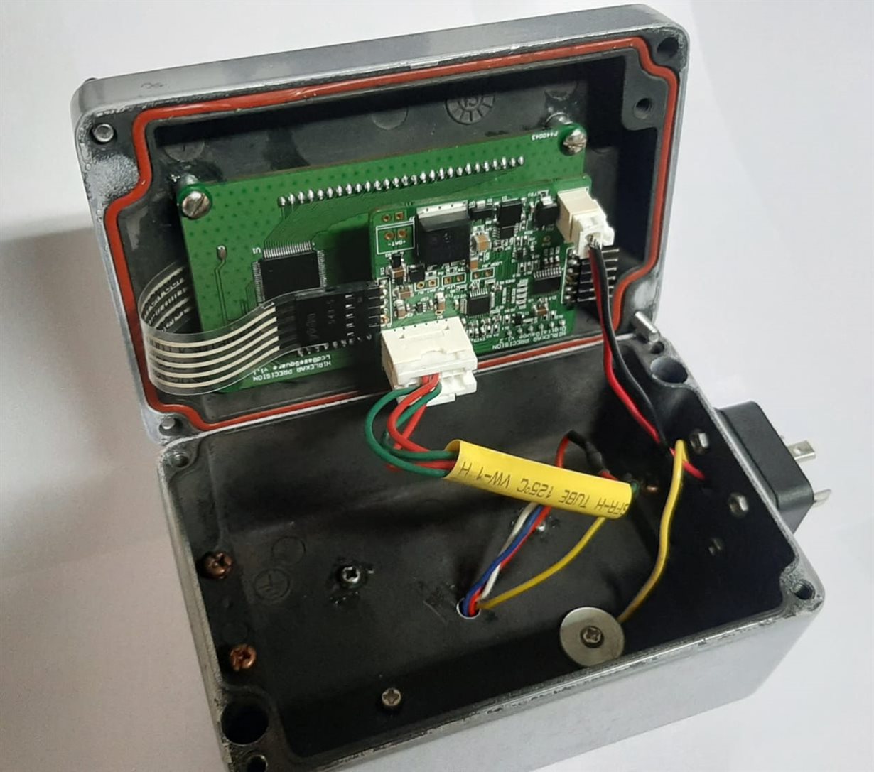
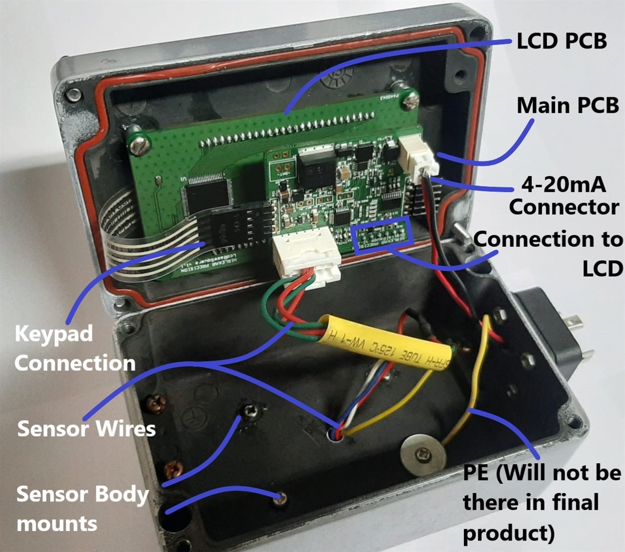
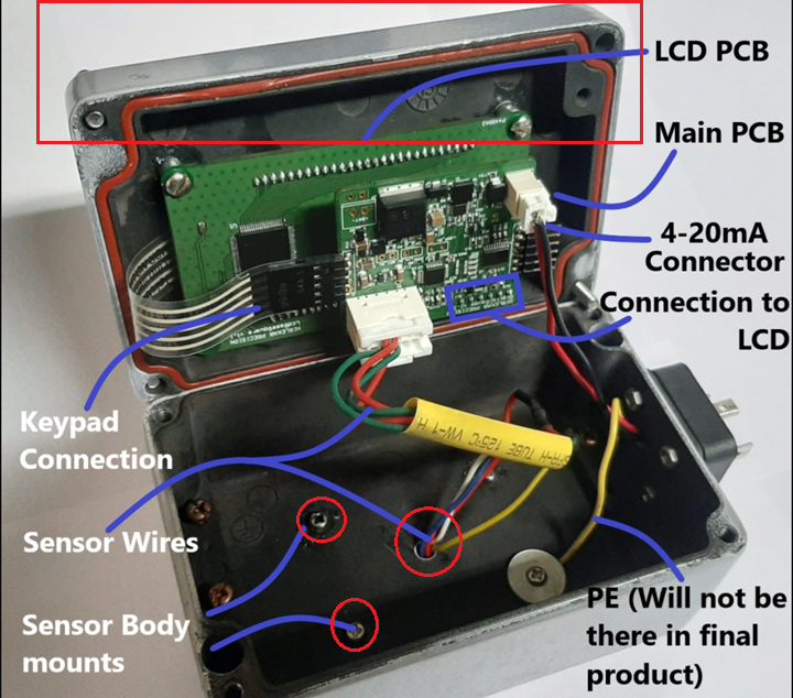
    can you please explain what we are seeing in the photos?

    Kai

  • We have a membrane keypad in the front whose pins goes to microcontroller directly, we also have cut out for segmented LCD display. On the side is the connector for 4-20mA output. In the back the black block is the sensor with its wire running directly in to enclosure.

    There was nothing specific that I wanted to show in the image but I shared them so you guys can get a better idea of the device construction.

    Apart from that i have mentioned the question I have in my last comment.

    "Few key take away I have found with respect to ESD, please correct me if I am wrong, is that the board and the metal enclosure forms a capacitor which protects the board by storing energy from the ESD capacitor and then bleeding the energy slowly. But it is not exactly working for us. So should we add a capacitor between local GND to the enclosure (chassis earth) wherever we have TVS diodes protecting the pins like LCD & keypad pins so the excess energy will not flow through XTR117 or should I also add the diodes arraignment as shown in Kai's earlier reply?"

  • Hi Yash,

    You are doing IEC 61000-4-2 Level 4 (Contact Discharge +/- 8kV; Air Discharge +/-15kV), where direct contact discharge is preferred and/or air discharge is used to locations that direct contact can’t be applied. The input pins of XTR117 are not part of this test compliance, especially when the input is directly exposed ESD waveforms.

    I believed that in the above ESD test, the EUT has to be configured as a standard installation unit, where the input is not exposed under this particular ESD test. In other words, you should not have an access to the internal pins of socket during the test, see the green rectangular shown in the image.

    From the images you sent, I saw the following potential issues.

    The EUT enclosure needs to be constructed similar to Faraday cage. The enclosure is coated with paint and organic protective films. If these materials do not have electrical conductive property, you may have issues at the mating area between LCD cover and base (left and right half of the enclosure).

    a)       The mounting side of EUT should expose with bare metal to ESD test table (the view is not shown in the image).

    b)       The paint or protective film should be removed to expose the metal surface between mating interface. If the gap is large or does not have full 360 degree physical contact (metal to metal), electrical conductive gasket or metal or EMI shielding fingerstrips/spring contacts need to be inserted between the gap.

    c)       The mounting screws should use stainless or Zn coated material (not FeO or black oxide type) between two LCD and base (It seems ok).

    d)       The base of input socket should be mounted on a exposed metal surface with electrical conductive gasket as mounting material. The gasket between mounting sockets should be conductive gasket as well, see the most left image in the large red rectangular.

    e)       The surface surrounding or underneath of the LCD panel should have same types of electrical conductivity to the enclosure. I am not certain that LCD panel and its surface are able to meet the particular ESD test and compliance.

    In terms of input protection in XTR117, you may try Kai's suggestions or try the following similar approach.

    If you have other questions, please let us know. 

    Best,

    Raymond

  • Hi Yash,

    the best measure against ESD is to shunt ESD arround the circuit and not allow ESD to enter the circuit. So the best cure is a Faraday cage (metal enclosure) with the ESD shunted onto this Faraday cage at every single point where a signal enters or leaves the enclosure. Shielded cables with 360° bonding to the enclosure help a lot by extending the Faraday cage over the signals entering or leaving the enclosure. And it's very important to make all cables enter or leave the enclosure at only one single point so that no path through the circuit from one end of PCB to the other exists!!!

    Can you share a photo which shows how the internal mounting and cabling are put into practise?

    Kai

  • Will respond soon :-)

    Kai

  • Yes, please do, we are waiting for your reply! 

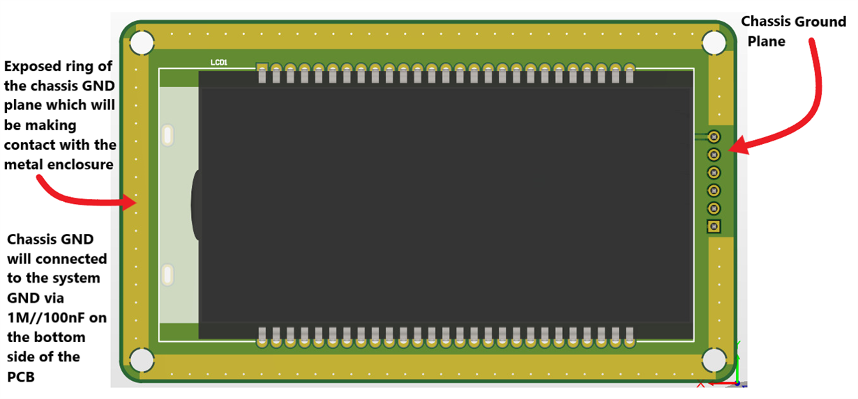
    In the next revision, we are planning to use chassis ground plane on the top where LCD is connected with exposed ring on the edge acting as guard ring. This ring/plane will directly connect to enclosure. Covering the LCD slot and making a faraday cage.

    We are adding 1Mohm resistor with parallel to 100nF capacitor on the other side of the board to tie the enclosure/chassis GND to the signal GND.

  • Hi ,

    Are you still having issues in passing the ESD compliance test? Or you would like to improve the your internal components layout for future references. 

    An EUT is being powered when ESD compliance test is conducted, at least this is how it is done in DO-160. A momentary ESD interrupt is allowed, as long as it is able to recover after the test. 

    An EUT's outer mounting surface is required to be conductive and placed on top of ESD testing surface or table. The inner surface of an enclosure also required to be conductive. If not, the connecting points such as screws and wire harness's output shielding etc. that needs to be connected to earth ground or terminate to a single known ground in the design. In practice, the EUT's outer mounting surface is the single ground termination to the entire system. In other words, all your inner ground connections should terminate to a single ground point, which that point should connect to the output mounting surface (called chassis ground).

    From your inner image, I see several potential issues,  if you are unable to pass the ESD compliance test. The comments are not in particular orders. 

    1.  I am not certain that inner black coating or spray is conductive. In practice, the inner spray or film should be conductive. 

    2. The interfaces of two half enclosures should not be coated. If it is coated, it has to be electrical conductive films or paint. 

    3. The O-ring is silicon type, and it needs to be conductive type or you need to place a conductive ring or seal when two half of enclosures are mated or locked. This is to extend the faraday cage.

    4. All interconnector pins (interface to outside environment) needs to have some kind of TVS clamps or high voltage protections that terminated to chassis ground.  If there is a HV path to pins when ESD test is conducted, it will discharge the ESD waveform to chassis ground asap. The cable outer harness should have a ground shield and terminated at the chassis ground as well. 

    5. If you are taken care all the precautions above, the inner electronic circuit PCBs should be pretty safe and able to pass the ESD compliance test. 

    6. The LCD display may be a tough one. You need to implement the same precautions that I describe above. You need to place a conductive seal or cutout metal spring/shield around the perimeters of the display, and mount and connect the LCD's ground plane/LCD's metal shield against the chassis ground of the cutout window at the inside of the enclosure. You need to extend the electrical conduction all around the LCD display. It won't hurt if you fill the LCD and enclosure gap with conductive epoxy or conductive adhesives to extend the faraday cage around the LCD's perimeters. 


    If you have other questions,  please let us know.

    Best,

    Raymond

  • Hi Yash,

    the problem is that you allow ESD to enter your enclosure, and worse, that you allow ESD to run through your circuit, and even more worse, across the PCB :-(

    This is the worst scenario you can imagine :-(

    I fully agreement with Raymond, you should entirely redesign your cabling. Mount the ESD absorbers (TVS) directly at the points where the cables enter the enclosure and shunt the ESD directly to the enclosure, either directly or via hybrid grounding ( through a 10nF cap). This has to be carried out for all the sensor cables, the output cables, the keypad connections and the LCD connections.

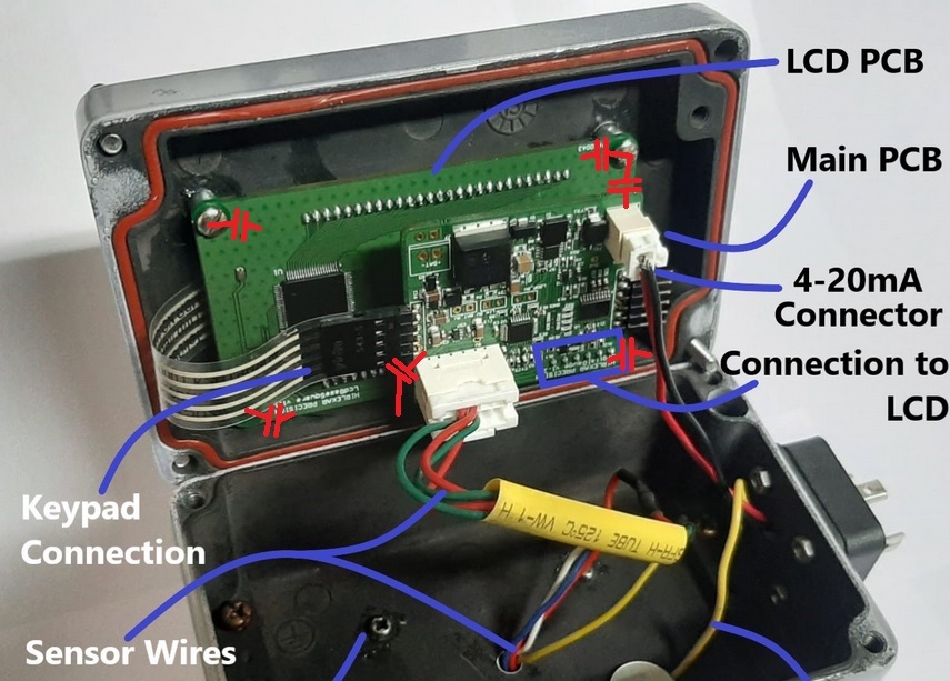
    As a qick fix you can try to perform hybrid grounding at the various points where the cables enter the main pcb and at the LCD pcb, like shown below:

    But this will only work, if all these signals have ESD absorbers (TVS) or low pass filters connected to the individual signal grounds (where the caps of hybrid grounding sit) to shunt the ESD into the ground plane and via the hybrid grounding caps to the enclosure.

    The best procedure is the method of "dirty box" / "clean box" which is discussed in every detail on this website:

    I'm very sorry to have to say this, but to put it very clearly, your ESD issues don't result from a bug or misconstruction of the XTR117, but from your vulnerable design.

    Kai