This thread has been locked.

If you have a related question, please click the "Ask a related question" button in the top right corner. The newly created question will be automatically linked to this question.

THS3062: How to calculate the power losses of op amp

Part Number: THS3062
Other Parts Discussed in Thread: THS3061, THS3121, TINA-TI, THS3122

Dear TI expert,

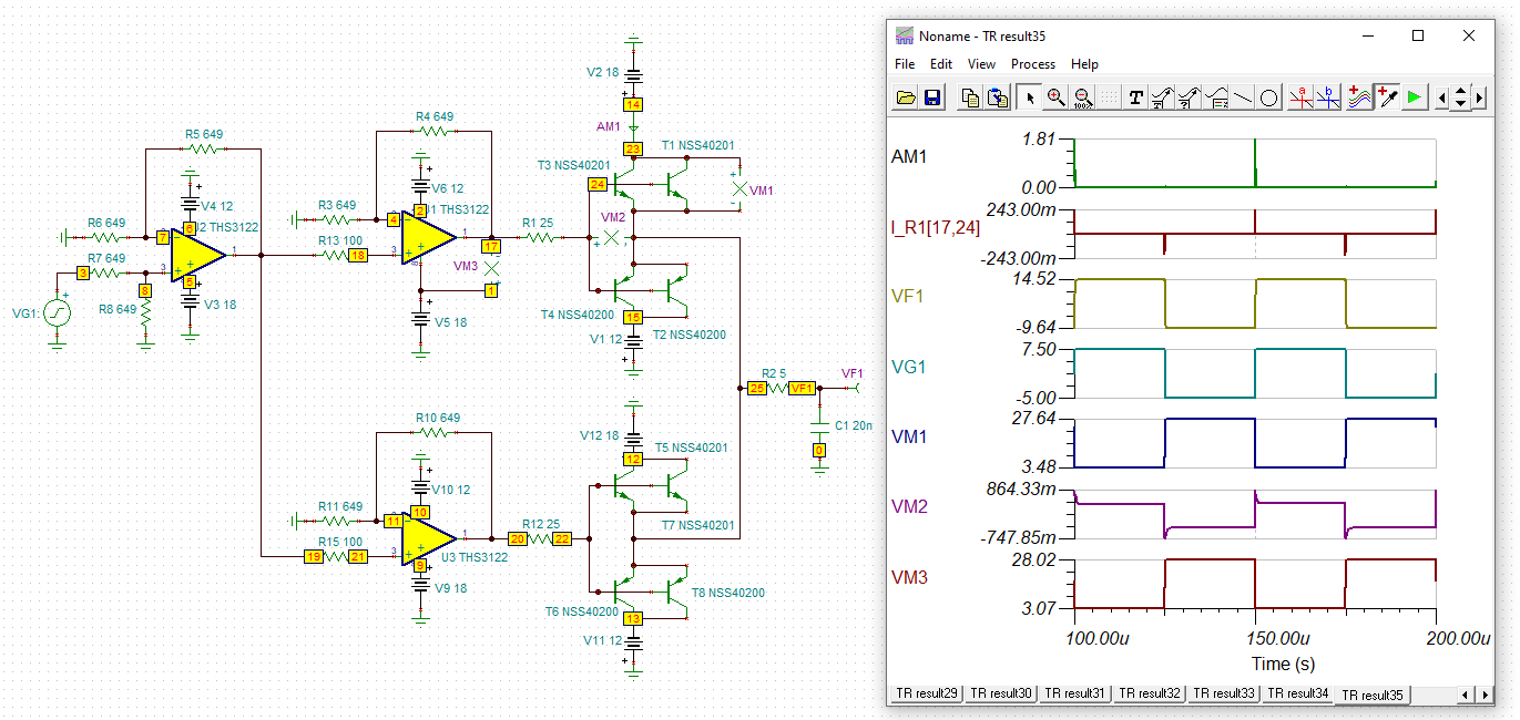
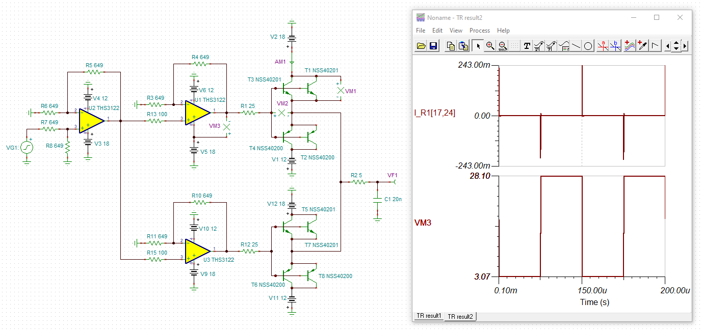
I use THS3062 to design the ckt as below. It is configured with gain=2. The amp is fed with periodic input of 20kHz frequency, with amplitudes of -5V and +7.5V. The output is then followed by a push-pull to amplify its current to drive a first-order RC ckt. The RC ckt has parameters of 5R and 20nF. Since the op amp has a gain of 2, the RC ckt is driven with a square waveform of amplitudes -10V and +15V.

Note that the op amp is not rail-to-rail, the op amp's supplies Vs+, Vs- are -12V and +18V respectively.

I worry that the op amp or the push-pulls (actually 4 in parallel with each other) may have too much power and then suffer from over heat or even damage. Hence, can you please show me how I can calculate the power losses of op amp and push pull in the ckt shown below.

Best Regards

Yatao

  • Hi Yatao,

    are these typical curves of your circuit?

    yatao_ths3062.TSC

    Kai

  • Hi Kai,

    Thx for your reply!

    Yes, this is my typical ckt, except that my NPN/PNP pair is ZXTN07045EFF/ZXTP07040DFF and the base resistance Rb for the NPN/PNP pair  is 25R.

    Best Regards

    Yatao

  • Well Yatao, 

    Most of your op amp power will be just the quiescent current - say worst case 12mA times 30V or 360mW and 2 times that if you are using the dual, 

    Kai's sims show a very high base current spike into the transistors, but a low static current - this is due to the very fast transition edges in the simulation. This current feedback device will try to follow that with its 7000V/usece slew rate - that high dV/dT will move the transistor capacitances very well but with that high peak current - if you don't need that kind of edge rate, slow down your input signal with an RC to the V+ input and it will reduce that peak base current on the edges. 

  • And with 25R base resistance the output current of THS3062 will very probably exceed the 200mA output current limit given in the absolute maximum ratings.

    Kai

  • Hello Yatao,

      As Michael said the typical power dissipation is easy to calculate when you have the quiescent current and voltage supplies. Here is an in-depth technical blog on calculating the maximum power dissipation. This blog takes in consideration of the current to the load as well as calculating the junction temperature. The maximum junction temperature for the THS3061 is 125C for continuous operation and 150C for abs maximum.

       Also, as Kai said, you would have to be careful with the output limitations of the amplifier. You can control the amount of current to these transistors by changing the base resistor. 

    Thank you,

    Sima 

  • Hi Kai,

    Sorry for the ambiguity, for simplicity, I've drawn only one THS3061 and one push-pull in the figure.

    In my real experiments, these are two THS3121(not 3061) in parallel and each of them drives 2 push-pulls. The total 2 op amps and 4 push-pulls together drive the RC load. 

    Also, in my experiments, the real input voltage to 3121 is generated by another op amp and edges of the input voltages Vi are not as sharp as the sims. 

    And my tests of tens of input pulses (Vi) show no wrong doings and RC load is driven correctly.

    But I have not done the continuous operations of this ckt, hence I ask you about the power losses of the op amps and push-pulls.

    Best Regards

    yatao

  • Hi Yatao,

    do you have a TINA-TI simulation file you can share with us? I happened to find Spice models of your transistors, but, unfortunately, TINA-TI refuses to accept them :-(

    Kai

  • Hi Kai,

    I have no such a file.

    If even you can not build such a file, I have no ability for sure.

    Can you please just give an estimation of the power losses? A rough value for my judgement of whether the ckt will break dwon in continuous operations. Thne, That will be enough for me.

    The spice files for the NPN and PNP are available at the right-side columns of the tables at "https://www.diodes.com/search/?q=ZXTN07045EFF&t=keyword&action_results=Go"  "https://www.diodes.com/search/?q=ZXTP07040DFF&t=keyword"

    Best Regards

    Yatao

  • Hello Yaatao,

       As Michael mentioned before most of the power dissipation will be the amplifier's power supplies multiplied by the max quiescent current of the amplifier. For the THS3121, lets say it is around 30V*11mA = 330mW. You will get a peak power dissipation in each amplifier at the maximum output current to the load (15V/25Ohm = 600mA) at the signal transitions shown in the sims below (Thank you Kai for the simulation, I only replaced the amplifier and base resistor). If you follow this TI precision Video on Power/Temperature for Amplifiers and/or its PDF Example, then at the peak output current, you will get a power dissipation in each amplifier between a maximum (DC) of around 2.62W and a maximum (AC sin wave) of 1.86W. This value will be towards the higher end near DC estimation. For calculating the temperature junction with a DGN-8 package (equation in video and pdf), you get a junction temperature of 152.82C to 178.2C (using DC estimation). Most likely, this probably will not reach these high temperatures, but it is better if we can increase the base resistor from 25 to atleast 45 ohms for DGN-8 and atleast 85 for D-8 in order to bring this junction temperature down to below Abs max of continuous operation which is 125 degrees C. 

    Thank you,

    Sima

  • Hi Sima,

    Thx for your reply.

    To make sure I understand you correctly, I wan to ask you does this sentence "you will get a power dissipation in each amplifier between a maximum (DC) of around 2.62W and a maximum (AC sin wave) of 1.86W. This value will be towards the higher end near DC estimation" mean: the peak instantaneous power of 3121 is 2.62W and the average power of the 3121 is still, as you say "For the THS3121, lets say it is around 30V*11mA = 330mW"?

    Best Regards

    Yatao

  • Hi Yatao,

    I tried to perform a more realistic simulation by changing the transistors and OPAmps. It turns out that the input signal rise time has a big influence on the issue of durability of components. The following simulations tell you everything you need :-)

    Firstly, an input signal rise time of 2ns:

    With zoom:

    Then an input signal rise time of 20ns:

    With zoom:

    And finally an input signal rise time of 50ns:

    And again with zoom:

    yatao_ths3121.TSC

    Kai

  • Hi Kai,

    I really thank you for your nice, patient support and valuable work for me.

    I measured the rising time of the VG1 voltage source in your post just now and it is about 10ns.

    How can I evaluate the power losses?

    Best Regards

    Yatao

  • Hi Yatao,

    let's discuss what's happening during the positive half wave of input signal. The behaviour during the negative half wave is nearly identical. The input signal rise time is assumed to be 50ns:

    As can be seen from the simulation "I_R1" is most of the time zero. Then no load related heat is dissipated within "U1". Only during the brief period when the input signal toggles high "I_R1" isn't zero:

    So for a period of about 70ns the heat

    VM3 x I_R1

    is dissipated within "U1". Calculate by hand this product with the help of the two cursors and you will see that the maximum power is about 4.4W, just when "I_R1" shows its peak.

    By other words: During 25µs - 70ns no load related heat is dissipated within "U1" and during 70ns a heat of up to 4.4W is dissipated. This gives an average load related heat dissipation within "U1" of

    < 4.4W * 70ns / 25µs = 12.3mW

    You have still to add to this dynamic heat dissipation the static heat dissipation caused by the quiescent current of THS3122 of up to 11.5mA which is

    11.5mA x 30V = 345mW

    Kai

  • Dear Kai,

    I replied to u that the rising time is about 20ns yesterday. But I think this will have little difference than the condition with 50ns.

    I will follow your calculation process precisely. But I wonder why the VM1 is across the positive supply and the output of U1, not simply the voltage across the U1 output and the ground?

    Best Regards

    Yatao

  • Hi Yatao,

    if you want to know what heat is dissipated within the OPAmp, you must take into calculation the voltage drop within the OPAmp, which is "positive supply voltage minus output voltage" for a positive half wave.

    Kai 

  • Hi Kai,

    Thanks for your explanations.

    But I think maybe the current flowing through R3 and R4 should be removed for the exact power of U1 :-)

    I am curious why you all think the quiscent current of 3212 is its maximum value listed in the datasheet?

    Best regards

    Yatao

  • Hi Yatao,

    to get the full heat dissipation of THS3122 the current through R3 and R4 would even have to be added, actually, as the current running through them also have to be delivered by the OPAmp and also create a heat power within the THS3122 :-)

    Kai

  • Also keep in mind, that there's an output current limit in the absolute maximum ratings:

    As the simulations show (see above) input signals with all too fast edges could result in a too high output current violating the absolute maximum ratings.

    Do you know the input signal rise time in your application?

    Kai

  • Hi Kai,

    The input signal rise time is around 10ns. Then this will affect the calculation results you give me?

    Best regards

    Yatao

  • Hi Yatao,

    in this case the THS3121 is in danger and the long term reliability will be degraded due to the violation of maximum output current specification. Then I would increase the two base resistors, as already suggested by Sima. Rb = 51R seems to be a good compromise :-)

    Kai

  • Hi Kai,

    Thank you for your help all the way.

    Best regards

    Yatao

  • Hello Kai,

       Thank you for these simulations and explanations! 

    Sima

  • Hi Sima,

    Thanks for your patient help!

    Best regards

    Yatao

  • Hi Michale,

    Thank you for your nice advice and your high levels.

    Best Regards

    Yatao

  • You are welcome :-)

    Kai