This thread has been locked.

If you have a related question, please click the "Ask a related question" button in the top right corner. The newly created question will be automatically linked to this question.

THP210: THP210 gain setting regarding

Part Number: THP210
Other Parts Discussed in Thread: THS4551

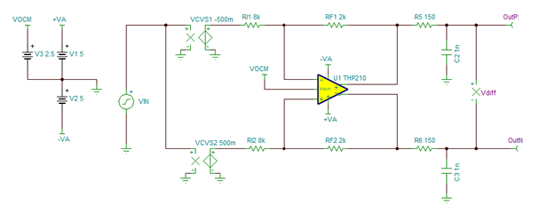
Whether THP210 shall be used to attenuate signal at 0.25 gain by adjusting feedback resistor?

For attenuation whether any specific config is required

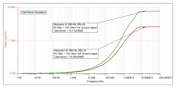
I gone through the datasheet, the unity gain FDA it recommends to use 2Kohm. Shall I use 1Kohm instead of 2Kohm.

If I use 1K what will be the impact. Request you to provide the solution for these queries.

  • Hi Malathi,

    As any amplifier circuit, there are trade-offs when scaling the resistor values of the fully-differential amplifier (FDA).  The component selection is dependent on the application requirements.

    Using the larger resistor values will increase the thermal noise contribution of the resistors, and increase the noise due to the input current noise of the amplifier interacting with the resistors. Nevertheless, the increase in the resistor values will also result in lower current consumption.  Smaller resistor values will result in lower noise, with a trade-off in the increase of current consumption. However, loading the amplifier with a load much smaller than 1kΩ will tend to start loading the FDA, and will result in an increase of distortion.

    Another factor to consider when scaling the feedback and input resistors of the FDA, is the input impedance of the FDA.  The input impedance is determined by the value of the input resistors, and therefore the designer needs to consider the drive capability of the preceding circuit or sensor driving the FDA when scaling the resistor values. 

    The THP210 offers the super-beta input bipolar transistors, that provide a reduction on input bias current, and a reduction of the amplifier input bias current noise. This lower bias current provides a reduction on the initial DC and drift errors in the circuit, and allow the use of larger resistor values with a relative smaller impact to noise, offset and drift errors.

    The datasheet tends to recommend 2kΩ feedback resistors, since this is a good performance compromise between noise, DC errors and power consumption.  However, if current consumption is not a major concern in your application, the THP210 is flexible and you can certainly choose to use 1-kΩ feedback resistor, providing a reduction in the noise.  For example, the datasheet tested circuit of figure 9-12 on section 9.2.2 uses 1kΩ feedback resistors and produces low noise and low distortion as shown in the FFT results.  In general, I tend to avoid using resistor values that produce a circuit load much smaller than 1-kOhm as they may start to load the fully-differential amplifier resulting in an increase in harmonic distortion.  (Note: A clarification on the figure 9-12, the input signal used to test this circuit was fully-differential). 

    The best approach to decide on the feedback and input resistor values for your application is to perform a quick total noise analysis of the attenuator circuit per the application noise, bandwidth, current consumption and input impedance requirements.  The THP210 TINA SPICE model can be use as a quick way to check the total noise, bandwidth and current consumption of your circuit so you can make a quick comparison.

    For example, the attached simulations for a very simple 0.25V/V attenuator(A), using RIN=8kΩ and RF=2kΩ with single-ended RC filters of 150Ω +1nF at each output offers a total output noise of ~15.04-µVRMS with a bandwidth of ~1MHz.  The load circuit seen by attenuator (A) is 10kOhm at each output.

    Attenuator(B), using RIN=4kΩ and RF=1kΩ with the same single-ended RC filter load at each output has a total noise of ~10.58-µVRMS with a bandwidth of ~1MHz.  The load load to each output is 5kOhm.

    Of course, this is just a quick example and there are many other better attenuator circuit configurations you can use.  For example, the attenuator and second order Butterworth filter circuit of figure 9-16 of the datasheet offers 100-kHz bandwidth and 0.433V/V gain. A similar circuit can be tuned per your gain/attenuation and bandwidth requirements.  Let me know if you have a specific bandwidth for the attenuator and we can tune a similar attenuator/filter circuit.

    Note: I should mention, the simplified behavioral TINA models do not model distortion since this is a complex transistor device behavior. However, you can choose to limit the minimum total load to a value to 1kΩ on the circuit, and still obtain low distortion performance.

    Thank you and Regards,

    Luis

  • Hello Malathi,

    There are performance advantages to keeping the feedback and input resistors used with the THP210 towards the lower range of values vs higher values. First, the thermal noise of the resistors is reduced with the lower value resistors. And second, making the feedback resistors lower in value avoids introducing excess phase shift in each of the feedback loops when that resistance combines with the THP210 input capacitance in each path. If the phase shift introduced by RF and Cin becomes large, then the phase margin will be reduced and instability could become a problem. 

    With fully differential op amps such as the THP210 an attenuator is easily achieved by setting each side of the amplifier up as an inverting gain amplifier having a gain less than -1 V/V. For the gain of -0.25 V/V (-12 dB) the input resistors just needs to be 4x the RF resistors. If each RF is set to 2 kΩ, then quite obviously each input resistor needs to be 8 kΩ.

    The THP210 is characterized throughout the datasheet with each RF = 2 kΩ, and a differential RL = 10 kΩ. Although you certainly can reduce the RF resistors to 1 kΩ, and then make the input resistors 4 kΩ the electrical performances can vary a little from what is listed in the Electrical Characteristics table and Typical curves. If you chose to do that the total resistive load on each THP210 output will be 5 kΩ, and that is in addition any differential load resistance and/or resistance to ground off each output. The THP210 outputs can drive up to about 15 mA each, but output swing to the rail becomes more reduced the more heavily the output is loaded (Figure 6-24. Output Voltage vs Output Current). Certainly it is best not to load the outputs any more than is needed in most any op amp circuit.

    Regards, Thomas

    Precision Amplifiers Applications Engineering

  • Well Malathi, 

    The points Luis and Tom make are very good, I also look at phase margin vs gain and Rf as well as noise and loading, Here is an article talking about these issues. 

    https://www.planetanalog.com/are-inverting-attenuators-with-voltage-feedback-op-amps-inherently-unstable-and-why-might-you-want-to-apply-them-insight-11/

    There is also a section in the THS4551 datasheet I wrote called designing attenuators you might find useful, 

  • Hi Malathi,

    I assume that the above replies have answered the question, however, please feel free to post if you have further queries.

    Thank you and Regards,

    Luis