This thread has been locked.

If you have a related question, please click the "Ask a related question" button in the top right corner. The newly created question will be automatically linked to this question.

[FAQ] INA199: Why can I exceed the absolute maximum voltage ratings if I am limiting the input current

Part Number: INA199
Other Parts Discussed in Thread: TIDA-00302, INA168

I really would like to use a particular current shunt monitor in my system; however, the input voltage ratings are a little lower than what is required.Fortunately there is a little footnote beneath the Absolute Maximum Ratings table that gives me hope that with some current limiting mechanism I may still be able integrate the desired current shunt monitor into my system. Can you explain why there is this caveat?

  • Texas Instruments offers a wide slew of current sensing options that are made such that they can be incorporated into many systems with different requirements.  As such, customers often need to evaluate trade-offs so that they can find parts to help them achieve the end goal.  In the process of selecting parts a customer may find a part with many desirable attributes yet also with some specifications that fall a bit short of certain design requirements.  Some may see these listed values as conservative and excessive safeguards that can be ignored with minimal harm and may even wishfully think they can observe similar performance with the device working outside of the recommended or even the absolute operating range.  One particular operating characteristic often challenging to meet system needs is the maximum input voltage. Accordingly, one might ask whether a device can be supplied with a voltage outside of specification and what are the consequences?  The answer is yes it can be done, but there is a catch.

    Many datasheets for current shunt monitors and sense amplifiers have a clause below the absolute maximum ratings table that reads, “Input voltage at any pin can exceed the voltage shown if the current at that pin is limited to 5 mA.”  With this there are two general scenarios, a transient spike in voltage outside of spec or a sustained voltage outside of spec.  A transient spike quite often is from electrostatic discharge (ESD) and can be several thousand volts.  Devices are expected to survive these events, and are outfitted with ESD diode structures or some other special internal protection circuitry to do just that.  Due to these diodes, the device often can technically still work after experiencing a voltage far outside of the recommended operating specification.  However, during the ESD event, the output will not function properly nor match behavior observed in the recommended operating range.  Also one thing to note is that ESD events may still cause unrecoverable damage as ESD events also have a maximum threshold defined in the datasheet and exceeding these will damage the device.

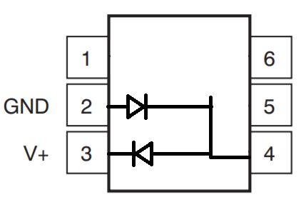
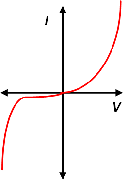
    A typical ESD diode protection circuit at a pin of interest has a diode forward biased to the supply and diode reverse biased to ground as seen in Figure 1.  Such a setup takes advantage of the diodes pulling a lot of current  in an overvoltage condition, with one diode strongly forward biased and another strongly reverse biased as can be seen in figure 2.   When these diodes start pulling a lot of current, the downstream circuitry that actually implements the chip’s function is starved of current.    While these diodes protect a device from a temporary surge, they do not protect the device from a sustained high voltage.  This is attributed to the heat produced from the diodes. 

    Long sustained voltages outside of the range specification with no current clamping mechanism will result in the ESD diodes heating up.  After sufficient heat is built up around the ESD diodes, the device will succumb to thermal damage with trace metals shorting, the device package melting, or the silicon structure being chemically altered.  Alternate overvoltage protection methods such as limiting the slew rate of the input to the device also have similar issues with heat.  These protection circuits are typically utilized on sense pins and are only intended for transient overvoltages.  Additional protection may be provided externally; a comparison of several external protection methods can be observed in greater detail in the TI reference design TIDA-00302. 

    Figure 1: Fundamental, typical ESD diode structure

    Figure 2: Diode I-V curve

    What generates the excessive heat when the input voltage is exceeded is actually more current which lead to more heat generated.  If the input current is limited or clamped such as figures 3 and 4 respectively, one might assume that all the problems are solved, but not necessarily.  The part will be saved, but the performance may not always produce desirable or expected results.  The addition of large resistors as in Figure 3 is not advised as it will affect the gain, gain error, and drift.  As for figure 4, this circuit and device are good for high side applications.  However, this implementation does exhibit linearity issues when the load current falls far below the average and max values expected (see table 2, section 4.2, tidu833).  Furthermore, if a high-side measurement is not absolutely necessary, this solution does add cost and additional board space as it requires several accompanying parts to operate properly, whereas a low side implementation with another device could be better.  Lastly, this solution can only be implemented with a few current shunt monitors that have topologies analogous to the INA168 that have a current output instead of a voltage output.

    Figure 3:  Limiting Current with Resistive Dividers

    Figure 4: Floating Device Ground to Create Positive Offset Input Voltage Range

    So knowing the tradeoffs of the above implementations, one might ask how to design one of the above implementations for their system.  First consider a design engineer has 100V power supply that needs a current monitor and has been told by management that price and board space are more important than accuracy.  While searching for a part, he realizes that no parts can directly take such a common mode directly.  He thus considers using figure 3’s implementation with a slick 26V common mode max device he found on TI.com.   His thought process is that series resistors R1 and R3 tapping the nodes of the current shunt will limit the current.  To do this correctly he takes the highest potential voltage on the part minus the lowest potential on the part, divided by 5mA.  So in this case he would take 100V-GND=100V; 100V/5mA = 20kΩ.  So putting 20kΩ resistors for RD1 and RD3 would be advised to account for all possible voltages present on the inputs flowing through the device to GND and limiting the current to 5mA.  For more information regarding this method, you may consider reading tech note sboa198.pdf (Extending Beyond the Max Common-Mode Range of Discrete Current-Sense Amplifiers).  As for the method in figure 4, the app note slla190.pdf (Extending Voltage Range of Current Shunt Monitor) gives brief description of the operation, while tidu833.pdf (High Voltage 12 V – 400 V DC Current Sense Reference Design) and tidu849.pdf (40 V to 400 V Uni-directional Current/Voltage/Power Monitoring Reference Design), give detailed reference designs for specific applications utilizing the implementation in figure 4.