This thread has been locked.
If you have a related question, please click the "Ask a related question" button in the top right corner. The newly created question will be automatically linked to this question.
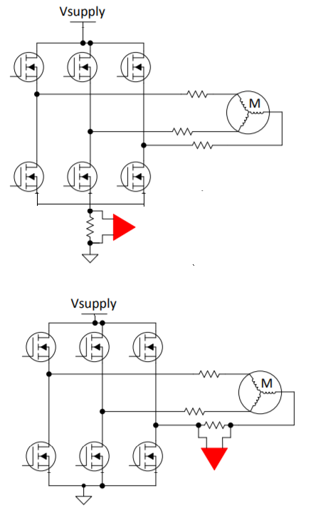
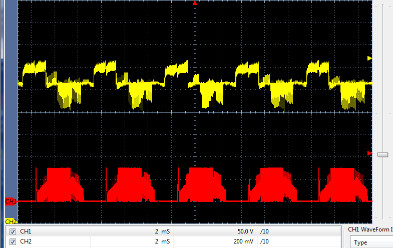
We are using the INA240-A2 in low side monitoring with +3v3 VS and the output is not symmetrical with trapezoidal waveforms being monitored. The PWM noise reduction seems better than INA282 in the same test circuit. Yet it would seem PWM rejection is not rejecting any such thing as 12.5Khz PWM pulses are very present on the output. It would also seem datasheets transient analysis differential IN+/- pins using a sine wave does not prove PWM rejection is even possible. Why datasheet have no graphs showing actual PWM rejection on output as only a square wave IN+/-, not an actual PWM signal to prove rejection?
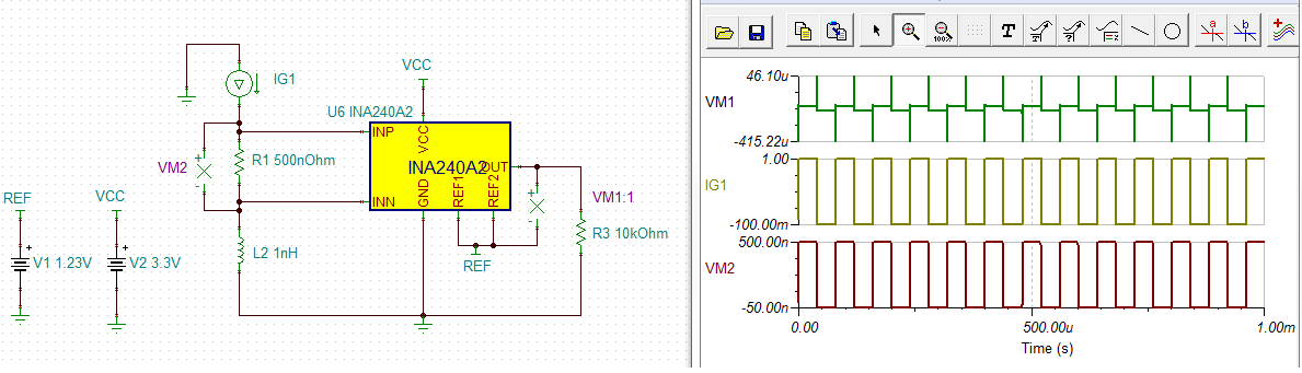
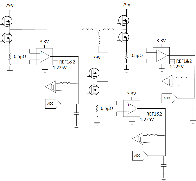
Forward positive current flow produces a somewhat monotonic output rise using 1.225v precision reference LM4041-N, REF1/2 tied together. It seems it can not produce a proper ratio metric or linear output rise from negative current thus produce (single) pulses in opposition to forward current having rise from 0v up to trapezoidal positive current peaks. The output signal losses symmetry when the PWM duty cycle rises above 25%. So differential amplifier bandwidth seems to increase in gain/db relative Figs. 10/12 for PWM frequencies 12.5Khz up to 40Khz. Tina transient analysis looks nothing like the output signal being produced.
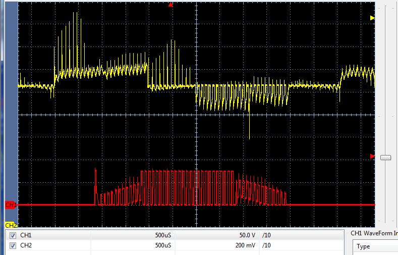
Previous testing circuits gave doubt of any proclaimed PWM rejection, we opted to add Johanson ceramic EMI decoupling cap XY2 1nf filtering on IN+/-. They made no difference in number of PWM pulses appearing on the output or the output gain exceeding well over 50 via 0.5uohm shunts. Whereas a 150 volt PWM pulse can easily produce outputs exceeding +/-2 up to +/-4v even tough VS pin has dedicated +3v3 regulator TPS735, VS pin 4.7uf/0.1uf bypass.
Why is there NO PWM rejection on low side monitoring and how can the A2 gain seem to exceed 50mv/A steady state duty cycles? Also seems excessive A2 gain error present, perhaps gain was not set properly at the factory or varies depending on the input signal type? What can we do to make the signal symmetry mirrored where SAR ADC can more easily determine ratio metric linear current rise in the PWM duty cycle?
Thanks for considering to use the INA240 in your design. So I want to clarify, you say you are doing low-side sensing which makes me think you would have an implementation like the one shown in the first figure below. However, you then mention negative or reverse current, which suggests you are actually doing in-line sensing like in the second figure. Can you provide a basic schematic or block diagram of your setup? From there can you provide a scope shot of the behavior you are seeing and indicate specifically where you are measuring at?
Hi Patrick,
Patrick Simmons said:However, you then mention negative or reverse current, which suggests you are actually doing in-line sensing like in the second figure
We are low side monitoring three 1/2 bridges. Logically bipolar switching current flows in both directions. That is to say PWM in slow decay the low side FETS are mostly saturated via 90% duty cycles and current recirculates in high side FETS each 80us period (slow decay). Perhaps also it depends on inductive inrush current in each 80us period where ringing at the beginning of each period seem to indicate electron pair waves cause reverse current flow and the INA240 can not settle fast enough even @400Khz bandwidth. Our Hantek 65 current clamp produces symmetrical output in series with phase, indicates balanced current flow in both directions exists.
So we since posting added TDK ferrite beads into the +3v3 VS source supply which seems to have stabilize the lower half of the differential amplifiers pulses. The signal is still not correct and should resemble the top half of wave. Instead the bottom part does not form bridges between pulses similar to the top half of the wave. Oddly only when the duty cycle is very low does the INA240 output produce symmetrical waves representing inductive current flow. That was the waveform behavior with or without Johanson 1nf EMI filter cap on the +/-IN or TDK ferrite beads. What else can we do to correct this behavior?
Hi Patrick,
Thanks for quick response and investigating this issue.
Patrick Simmons said:On a different note, we suspect your scope may also be amplifying the magnitude of those transient peaks you see.
Sadly the +/- output spikes are present and can easily trip the analog fault comparator cutting off PWM drive. The A2 50V/V is randomly producing roughly 100mv/A with 0.5uOhm shunt and seems to reduce if the output is divided below REF1/2 voltage threshold (1.65v). Doing so requires 523R resistor to ground in output divider which allows PWM noise to plague the samples. So this time we opted to stay below 1.65v using 1.225v direct into REF1/2 with no divider on the output, producing floor threshold bit higher than the dividers 540mv floor. The 1.225v REF1/2 should produce around +83A full scale and arrest INA from spewing so many pulses below ground, that has not worked out so well. The layout is highly flexible designed for summation, first INA sets REF1/2 threshold of second. We are only using one INA and bypass 2nd via solder bridge REF1/2 pads to output pad. So the 2nd INA for summation is not populated at this time.
Patrick Simmons said:We expect the settling time to be around 9.6us. So with a 80us period, I calculate the PWM high duration as 72us and that would give you a max recommended sampling duration of 62.4us.
Actually the PWM ringing settles within 1.5us and we fire one shot timer delaying sample window, roughly 2.5us with 1.5us conversion latency using 2x oversampling producing 1.14MSPS digital representation of the captured samples.
7-14-18 (We trusted the ADC was capable of sampling 2MSPS but was actually 1MSPS)
So the INA output impedance and REF1/2 inputs obviously have little noise rejection, larger part of the issue. After adding ferrite beads to the REF1/2 source regulator & output reveals a new artifact that was missing when the CMM slope changed relative to the duty cycle.
We order the B102C/B601C may further reduce ADC input impedance and stop random spikes of IAN output from attacking MCU busses.
Hello BP101,
The behavior you are observing we believe is due to parasitics and possibly how you are taking your measurements. With respect to discussing the impact of parasitics and proper setup, I think this FAQ does a pretty good job. Although it is written for reducing output voltage ripple on a buck regulator, I think the concepts are still relevant. As there still may be other contributing factors, I am still researching your issue. If I find other possible explanations or a fix, I will let you know.
You mentioned that the pulses could trigger your comparator. From the peaks you have measured, I understand your concern. After ruling out any peak transient contributions associated with your measurement setup, these peaks may still be present. However, we believe that these peaks may be short enough in duration such that the parasitic input capacitor to your comparator may not be sufficiently charged to the trigger point. Additionally, a filter can be installed such that it only trips for faults that last longer than these switching transients that you are observing.
The odd part is pulse peaks often seem to exceed 50v/v gain, act more like 100-200v/v gain. Again 5uohm shunt requires scope current probe 50mv/A for comparable current measures to other current measure instruments. Long ago calculated 25mv/A for *50 gain with 5uohm shunt. Also a 5mohm shunt produces more output gain, one reason we lowered input +/- IN to microvolts by reducing shunt size. These captures are not showing cyclic surge peaks occurring on the INA output often exceeding far -2v below ground and above +3v3 VS .
These captures show the output gain is far from being 50v/v with a 5uohm shunt. It would seem even with the INA282/50v the gain was not being set as stated. Point is adding a voltage divider on the output to effectively lower the gain also effects the currently measurement. E.G. INA240A2 with 1.225v REF1/2 and 0.5uOhm shunt should produce 500uv/Amp*50gain=25mv/amp. Yet it produces twice the gain or 50mv/A and not 25mv/A as expected for 50v/v gain.
The datasheet example showing formulas for shunt selection divides the output gain when it logically should be multiplied as current gain on the amplifier output. What is with division and why the excessive gain?
Hi Patrick,
Thank you for checking on this issue but really something is not right with either gain or conditions causing gain to jump. The principle behind the INA series is to reduce parts count and precision required for OPAMPs preforming the same typical low side current measures.
Patrick Simmons said:The behavior you are observing we believe is due to parasitics and possibly how you are taking your measurements. With respect to discussing the impact of parasitics and proper setup,
Well these peaks (capture) represent inductive inrush current beginning of each 80us period. Current leading the voltage causes ringing in the inductor until saturation point, reason for X2Y EMI 1nf filter on +/-IN and MMZ ferrite bead on the output.. That is not NFET (di/dv/DT) or Qrr recovery since that occurs below ground or slightly above but never at peak VDS.
Again the INA output gain is not what it should logically be for 5uohm shunt and falsely represents current measured as a micro voltage of said shunt. Also fails to produce very little ratio metric rise if REF2 is below +1.65v or REF1 GND as VS=+3v3. So the entire current measure INA240A2 is plagued in this REF1/2 1.22v configuration unless the differential amplifier output signal is divided down to 450mv with REF1 +1.65v REF2 GND. Tina transient analysis is not showing same output peaks with a similar PWM inductive load and REF1/2 +1.225v VS=+3v3. So something is really not as it should be and from my experiments it seems the amplifier gain is not being set correctly at the factory.
Accordingly TI-Tina transient analysis INA240A2 produces closely to that signal output on test bench. Accept for the negative 1/2 cycle pulses and the unexplained repeating +/- pulse surges, zoomed in makes sine wave result of pulse peaks. That has been an ongoing issue of INA240/282 in every inverter tested so far, the output oscillates in random AC wave pulse peaks no matter if capacitance is kept below 1nf. The Johanson X2Y EMI input capacitor Excel calculator is a bit behind and the CMMR versus Frequency graph Fig.12 when input 15mm steps produces a non monotonic arc in the first graph (see attached). Also the proper output impedance matching to SAR ADC is a must but that value is no where to be found in INA240 datasheet.
Let me add the 1st capture in this thread would incorrectly suggest an 15-20 amp phase current peaks, other test instruments more realistic report 2.6 - 3.0 amps @80vdc. Again scope current probe reports 50mv/A to match the typical phase current of other current measure instruments.
Otherwise current above capture from scope thus measures 6-12 amps on 25mv/A probe setting showing in digital Min/Max/Peak readouts. That may just be X10 probe on INA output required X1 probe channel to reduce 50mv/A but all three instruments can't be wrong. That's why it seems the output gain doubles as if REF1/2 are not dividing output gain symmetrically so the full 50v/v ends up as very high positive/negative pulse peaks. Gain should divide 25v/v up and 25v/v down not produce 50v/v in both current directions.
We thus subtract +1.225V (REF1/2) from the output amplitude to derive 25mv/A in software calculations. Then dividing the analog voltage from the INA240 relative to duty cycle in the ratio metric liner rise.
Hello BP101,
I apologize for the delay in my response. There a few reasons we think measurement setup can be an issue. As you are using a low-side implementation we only expect the common mode voltage to fluctuate a few tens of mV. As for the device gain, it corresponds to trimmed resistors calibrated at the factory. Based off of our Gain bandwidth plot we expect the gain to be relatively constant up to a couple 100 kHz. Beyond those frequencies we expect the gain to decrease and eventually attenuate the signal. Those transients you are observing correspond to the rising falling edges of your PWM signal which can be decomposed of frequencies significantly higher than 12.5 kHz. As such we do not expect the INA240 to be amplifying those. However, we do think that there is ground coupling that is allowing those transient pulses to express themselves at your output. Below, I illustrate the concept with a TINA model. In this case I just have a parasitic inductor from the shunt to ground. In reality, you could expect this inductor at the device ground as well as the output. However, for this particular model it does not matter. One thing to note, this TINA model is not the Cadence model. It is a very simplified model of the part, best used for DC analysis.
As you have your reservations about our proposed reason. We definitely can test your circuit on the bench. At the moment, I think your circuit looks like the following figure below. Please correct me or fill me in on any details I am missing. If you would rather not share this on the forum, let me know below. I will send you a request through the forum to share details through email.
Hi Patrick,
Thanks for responding and do understand being heavily tasked.. Can PM the schematic part if you still need it.
Patrick Simmons said:Based off of our Gain bandwidth plot we expect the gain to be relatively constant up to a couple 100 kHz.
We are seeing 10-19Mhz ringing only after low/high voltage peaks occur. It seems the REF1/2 tied together may be doubling output gain during HV events (110v) peaks and 185v previously added output divider. Note again we do have X2Y 1nf EMI filter on the INA +/-IN and trying to get a Spice model from Johanson. We did not enter all the graph data on the first tab (lower db values), seemed futile requires 2R minimum and last tab automatically forced 2k series resistors in the filter.
There is so much gain error in the spikes eventually trips the analog fault comparator (VREF pot set 2.8v threshold) infers 112 amp spike trips fault when GUI current digital reading 4.8-5A. We had previously configured INA240A2 for 500uohm shunt but divided the output series 1k, 523ohm to ground. That divider lowered (REF1 +1.65v) output to 540mv (REF2 GND), was the only way output spikes were not tripping fault but at a much lower comparator fault trip threshold 1.79v.
BTW: Your model has 500nohm shunt and ours has 500uohm shunt. Can you test transient results for 500uohm shunt to see any difference?
Hi Kia,
Perhaps not as INA240 has advanced PWM rejection to stop (ΔV/Δt) on the +/-IN. Adding input filters is discouraged in datasheet text.
Datasheet quote:
Enhanced PWM rejection provides high levels of suppression for large common-mode transients (ΔV/Δt) in systems that use pulse width modulation (PWM) signals (such as motor drives and solenoid control systems). This feature allows for accurate current measurements without large transients and associated recovery ripple on the output voltage.
Patrick above states as db/frequency increases beyond bandwidth the differential signal is attenuated (reduced), not increased. So the narrow pulses you speak of should not be peaking so high if the pulse frequency is 9-10Mhz or greater.
I find it more interesting the output gain seems to produce 50mv/A, should be closer to 25mv/A. That alone judging from external current test instruments the output gain seems to peak near 100v/v, far from 50v/v. Perhaps one reason why we are easily seeing output pulse peaks exceed 75 amp full scale. Even after accounting for -200mv swing from +3v3 supply rail, hard to believe that being simply REF error. Oddly the TIDA-00909 engineers chose A1 gain (20v/v) and split REF1/2 mid supply. Seemingly they were aware something ain't right with INA output gain. Oddly TIDA-00909 technical analysis PDF states 7ARMS (10-A peak) per phase, yet AC induction motor 120 degree slip commutation phases all turn on together, seemingly exceeding 10 amp full scale listed. Phase current in our system occurs from 2 phases commutating at a time in 120 electrical degrees, 75 amp full scale.
Hi Patrick,
Patrick Simmons said:However, we do think that there is ground coupling that is allowing those transient pulses to express themselves at your output.
Most the pulses you refer to be ground noise in capture are actual PWM pulses (transient response) trigger scope on each 80us rising edge that at times peak near or above 110vdc and ring 9-10Mhz there after. It seems to be relate to the inductor current in some way but revolves in cycles when scope horizontal is set to scan or a very slow time base, zoomed out.
BTW: Modified X2Y Excel calculator closely follows INA240 CMMR graph figure 12. The filter seems to require 50 ohms minimum series R to for 1.2n X2Y input cap with 1mv error. Not sure how that relates to 50uv/A shunt we are using - just yet. The (Error_Xcap) tab pink cell error frequency is only an example, enter the error values for your desired PWM frequency!
Updated:7-17 7:59 AM EST
Below an older capture low side shunt (5mohm) reveals CMM peaks 375mv. Captured via 2 probes on shunt, 2 channel multiplication. Reveals typical shunt CMM symmetry is being distorted by the instrumentation amplifier output. The amplifier output (first post) is non-ratiometric, distorted and full of transient pulses relative to the saw steps captured across the shunt. The saw steps appear to drive differential amplifier transient response gain beyond datasheet CMMR specifications. Reducing shunt value by factor 10 to 5uohm lessons the effect in transient response to saw steps but it is still non the less present beyond figure 12 of datasheet.
INA282 has same issues with stepped shunt transients causing large swings in output gain. The 240 PWM rejection cleans up the output mess we noticed in the low side monitor 282. Yet 240 still produces overly large gain pulses that distort the amplifier output relative to actual current measurements.
Perhaps the differential amplifier design in both current monitors has an issue with stepping transient response relative to DC supply rail noise. It seems the saw steps of PWM pulses can produce output gain issues even at 400kHz bandwidth.
Filtering 240 REF1/2 supply via MMZ1608B102C (1k) ferrite beads 100n to ground seems to have limited effect. Where 25mv/A can barely qualify as having any accuracy among the barrage of differential amplifier output pulses, exactly 80us to the 12.5Khz PWM noticed upon DC supply rail. It would seem the INA series has little DC supply (VS/REF1/2) isolation barrier from the differential amplifier perspective. Datasheet supply side noise rejection graphs seems to take stance the DC supply is noise free, no PWM!
Perhaps a larger issue with low side monitoring than inline phase as -/+IN is then (isolated) away from lower voltage VS/VREF1/2 PWM noise. The INA series datasheet graphs appear to ASSUME no PWM frequency is present on DC supply. There needs to be (illustrated datasheet workarounds) for customers to install proper DC supply isolation for VS/REF1/2 pins of the INA series amplifiers. The conditions surrounding current monitor placement demand LAB provided examples of how to counter outside effects of PWM upon VS/VREF1/2 inputs, not simply pretend PWM rail noise don't exist at these inputs!
HI Kai,
kai klaas69 said:Sorry, if I sound old-fashioned, but I cannot imagine that a 400kHz OPamp can handle these nasty, huge and narrow spikes exceeding so much the 400kHz bandwidth
The point is 240A2 is amplifying low level PWM pulses from other than the shunt signal when it should be rejecting or ignoring relative to the quiet shunt signal posted above.
There are no such transients present in the shunt wave form capture yet they are present on the output. Comparing INA282 10Khz nominal bandwidth output signal was not much different though pulse amplitudes were much lower being REF1/2 the RVRR (+/-25uv/v Min, +/-75uv/v Max).
The high pulse amplitudes 1st post capture are due to 240A2 RVRR (2uv/v) thus amplifying 12.5kHz riding on the non-inverting amplifier input. There is low level 12.5Khz riding on +3v3 LDO supply to VS pin also feeding LM4041n +1.225v for REF1/2. The RVRR being very low at 50v/v and 20uv/v A1 @20v/v has better noise rejection. That is the troubling part being differential amplifier no matter the bandwidth will distort the output signal if PWM pulses enter VS or VREF pins. That fact should be know by the TI experts and not simply fly under the radar! Outside signals must be decoupled from VREF/VS pins and include datasheet examples how the LAB accomplished that before marketing these IC's in the way they have.