This thread has been locked.

If you have a related question, please click the "Ask a related question" button in the top right corner. The newly created question will be automatically linked to this question.

TINA/Spice/OPA377: OPA377 Input Offset voltage impact and simulation

Part Number: OPA377
Other Parts Discussed in Thread: TINA-TI,

Tool/software: TINA-TI or Spice Models

First of all, thank you for the TI Precision Labs! Really helpful.

Spoiler: As I was writing this question, I believe I found the answer...

I would like to confirm the impact of Vos to my circuit, simulate it if possible and eventually, to obtain a transfer function.
OPA377 simulation confirms the typical datasheet values. (See TI Precision Labs - Op Amps: Vos and Ib)
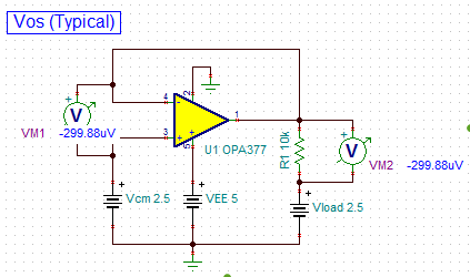
Following  suggestion (see related question) I inserted a voltage source in series with the positive input terminal of the OpAmp.

The circuit shown here is the superposition simplification of the circuit of interest, which only includes Vos.
As the gain is expected to be 1+(6.8k/200) = 35; I thought I would expect 35mV, but as you can see, the simulation shows 25.82mV

Then, I realized, this simulation model requires approximately 300uV to drive the output to Zero, thus I decided to run a "Vos" sweep, between -1mV and 1.3mV.

As expected, because my power rails work between 0 and 5V, I see "zero" until Vos is greater than 300uVL and I see 36.2mV output at 1.3mV Input

Questions

  1. Could this confirm my assumption that the Vos impact would be given by the following simple formula: Vout(Vos) = (1+6.8k/200) * Vos
  2. Why do I see a slight difference: 36.2mV (simulation) vs 35mV (Theoretical)

Thanks!

Alberto

  • Alberto,

    You are correct, the influence of offset voltage in your non-inverting amplifier is the same as the gain equation for the circuit. It's relatively easy to see its influence in this circuit since the offset voltage is added directly in series with the input signal. As you have discovered, TI's macromodels generally include a built-in offset voltage that is approximately equal to the typical offset voltage of that particular op amp. You have added to that offset with your additional 1mV test input offset voltage source. Don't forget, offset voltage could be positive or negative. In your case, the two appear to add.

    The total effective offset in a particular circuit can include other possible error sources. These primarily include:  1) Input bias current  flowing in source resistance.  2) Finite open-loop gain.  3) Common-mode voltage rejection effects. Checking the specifications of your selected op amp, the first two effects are likely negligible in your circuit. The additional offset in your case is likely due to common-mode voltage. The input voltage of your circuit is skewed all the way to the negative supply rail (ground, in your case). When the common-mode input is skewed away from center (between the supply voltages of the op amp), additional offset may be induced. The typical CMR of this op amp is 90dB or about 32uV for each volt skewed away from center. The numbers don't work out exactly, probably because the macromodel is not exactly matching the typical this common-mode voltage effect.

    All this raises interesting topics for a future blogs. Oh wait...  I'm retired!  Never mind.  :)

    Bruce

  • Hi Bruce. We are lucky to have you around, even after retiring ;)

    I racked my brain to figure out the CMR impact you mention (32uV), and I now remember comes from ΔVos = ΔVcm*10^(CMRR(db)/20)

    https://e2e.ti.com/blogs_/b/analogwire/archive/2013/10/14/what-you-need-to-know-about-cmrr-the-operational-amplifier-part-1

    The thing that threw me off was "The typical CMR of this op amp is 90dB or about 32uV for each volt skewed away from center"...

    I then remembered I had seen a formula explaining how to calculate the CMRR error and... now it makes more sense!

    https://training.ti.com/getting-started-current-sense-amplifiers-session-9-understanding-common-mode-voltage-error?cu=456802

    Thus, if I am measuring in the range of 0-100mV, assuming a gain of 35, I should expect an error at the output of 2.4V x 32uV x 35 = 2.68mV

    Thank you for this. This has been really helpful.