This thread has been locked.

If you have a related question, please click the "Ask a related question" button in the top right corner. The newly created question will be automatically linked to this question.

Circuit for ultrasonic threshold detection

Other Parts Discussed in Thread: TINA-TI, OPA2320, OPA2350, OPA320, TLV2460, TLE2426

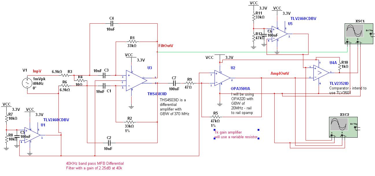
I have designed the attached circuit for detecting how long an ultrasonic pulse need to to travel a distance. the input signal is going to be from a 40 k ultrasonic receiver. First stage is 40k Band pass - 1k pass band - differential MFB filter with a gain of 2.25dB at Center frequency. In feedback path of differential amplifier I have used 33k instead of ideal value of 31.6k . I will appreciate some useful comments on how this circuit can be improved. Also I am going to design a PCB using smt components. I need suggestion to improve the circuit like adding capacitor to supply rail and VOCM which will reduce power supply noise etc.

regards

Ajit Singh

  • Hello Ajit,

    Your circuit is straightforward; however, a few changes may help you better achieve your performance goals:

    • The TH4503 does provides the necessary minimum gain-bandwidth (GBW) required to support your filter requirements. The effect of using the 33k resistor will increase the gain slightly and move the center frequency down by a small amount. You can see the affects if you simulate the filter using TINA-TI. I can't help but wonder why you chose to use the 33 k 1%, when 31.6 k 1 % is a standard value too.
    • I am concerned with attempting to get a gain of 1000 v/V at 40 kHz from a single stage. The OPA320 does not have sufficient bandwidth to supply that gain at 40 kHz. I suggest dividing the gain up equally between two operational amplifiers in a dual amplifier (OPA2320). The OPA320 appears to have about 55 dB of open-loop gain at 40 kHz and each stage would need 29.5 dB of closed-loop gain - so there isn't much loop gain left. The OPA2350 has about 5 dB more gain at 40 kHz so two stages may come closer in developing the 1000 V/V (60 dB) closed-loop gain you seek. A higher gain-bandwidth operational amplifier may be necessary.
    • You will need to place an effective bypass capacitor path at each of the points where Vcc and the 1/2 Vcc voltage connects to the operational amplifiers. These need to appear as a very low impedance at the frequency of interest. See the data-sheet for each amplifier you have selected for power supply bypass capacitor details.
    • The TLV2460 operational amplifiers that drive the 1/2 Vcc lins may become unstable (oscillate) if the capacitive load on their output becomes too large. A device that is designed to provide the 1/2 Vcc function, eliminate the need for two matched resistors, and will drive a wide range of capacitance is the TLE2426. There is a small possibility of oscillation under a certain load condition, but for your circuit doesn't appear to be an issue (Fig 17 in data-sheet).
    • I don't know what filter synthesis program you used for the filter, but I do note a discrepancy in one component value when I check the circuit using TI's FilterPro. The input resistors (R1) are shown in your schematic as 6.9 k. FilterPro produces a value of 12.28 k. Possibly, one of my assumptions about your filter response is incorrect.

    I hope this helps.

    Regards, Thomas

    PA - Linear Applications Engineering

  • hello Thomas

         Thank you for your response. I have designed this circuit using NI Multisim. i have used 33k as i don't have 31.6 available in my lab. a gain of 1000 was for worst condition. I hope i will not require more than 200 at worst. i wan't to reduce stages at this will add to the latency. Some delay would be introduced by each stage of amplifier. one clarification regarding TLV2460 oscillation. Is the oscillation would be due to bypass capacitors? I was not aware of TLE2426 kind of component.

    Thank you

    Ajit Singh

  • Hi Ajit,

    The power supply bypass capacitors that you place on the 1/2 Vcc output level appear as a capacitive load to the TLV2460 output. Adding a bypass capacitance with common values of 10 nF,100 nF, or more, is considered a large capacitive load. The capacitive load, in conjunction with the amplifier's output impedance, result in a pole that adds additional phase shift to the feedback loop. This reduces the phase margin and if at some frequency the margin goes to zero degrees and the amplifier gain is great than 1 V/V, the circuit becomes an oscillator.

    Different operational amplifier models will have a different phase margin at the unity-gain cross frequency and their output impedance vs. frequency can be very different as well. Both are significant factors in determining whether a particular operational amplifier will be stable when driving a capacitive load. You can usually find a graph in an operational amplifier's data-sheet indicating phase margin vs. load capacitance, or overshoot vs. load capacitance that will provide a good indication of stability.

    Regards, Thomas

    PA - Linear Applications Engineering