This thread has been locked.

If you have a related question, please click the "Ask a related question" button in the top right corner. The newly created question will be automatically linked to this question.

LM311 and LM339 for zero crossing detector

Other Parts Discussed in Thread: LM311, LM211

I'm trying to build a 100kHz sine-to-square converter by implementing zero crossing detector circuit using comparator.

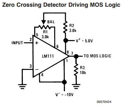
I used following circuit in LM311 manual

I get the following response:

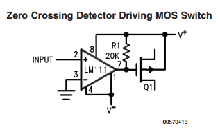
I also tried this circuit

and I get this response:

Both circuit are recommended in TI manual: http://www.ti.com/lit/ds/symlink/lm311-n.pdf

I can understand that LM311 is slow and it has long propagation delay.  But I don't understand where does the asymmetry come into play.  Is there a mistake in the circuit?  I'm using +/-5V supply voltage, except for the -10V in the first circuit as indicated on the drawing.  

Thank you very much for input and help.  I really appreciate it.  

Best,

Charles

  • Hello Charles,

    When the output is low, the LM311 output transistor is on. Notice the quick response to the low output voltage.

    When the output is high, the LM311 output transistor is off. The slow slew rate going high is set by the output resistor and the capacitance on output node. The time for the output to rise 63% is R*C. The rise time can be decreased by lowering the output resistor (R3 in 1st schematic, R1 is 2nd schematic). 

  • How low do I need to reduce the resistor?  What do you mean by output capacitance?  I would like it to be as symmetric and fast as possible.   Thank you very much!

  • The output capacitance includes actual capacitors on the output pin node, oscilloscope cables/probes, and MOSFET gates. The total seems to between 200pF and 400pF.

    The resistor needs to limit the LM311 current to 50mA or less. With 10V that is 200 ohms or greater.

  • Thank you very much Ron.  

    I tried to reduce the resistor and it does make the slew rate faster.  

  • I'm not sure why the +5V and -10V are used as supply voltages. My inputs will vary from +15V to -15V and will drive 3.3V  logic.  Do you see any problems with the circuit below. It simulated fine but it isn't like the zero crossing circuit in the example.


  • Let me correct myself.  My supplies are +/-15V and the input to the LM211 is +/-12V.  So VID is met.   Another question is about the ground at the non-inv input and the output ground.  If i use an analog gnd for the input and a digital gnd for the output, would that work?  Then to add hysteresis, I will add a resistor between the output and non-inv input?

  • Peter,

    You could use both grounds if you wish. The hysteresis resistor is placed where you said.